

166
Digital Electronics
logic status of the inputs. This variation in output impedance occurs owing to the varying combination
of MOSFETs that conduct for a given input combination. All buffered devices are designated by
the suffix ‘B’ and referred to as the 4000B series. The 4000-series devices that meet 4000B series
specifications except for the V IL and V IH specifications and that the outputs are not buffered are called
unbuffered devices and are said to belong to the 4000UB series.
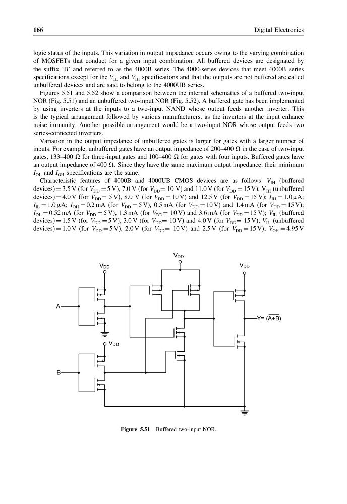
Figures 5.51 and 5.52 show a comparison between the internal schematics of a buffered two-input
NOR (Fig. 5.51) and an unbuffered two-input NOR (Fig. 5.52). A buffered gate has been implemented
by using inverters at the inputs to a two-input NAND whose output feeds another inverter. This
is the typical arrangement followed by various manufacturers, as the inverters at the input enhance
noise immunity. Another possible arrangement would be a two-input NOR whose output feeds two
series-connected inverters.
Variation in the output impedance of unbuffered gates is larger for gates with a larger number of
inputs. For example, unbuffered gates have an output impedance of 200–400 in the case of two-input
gates, 133–400 for three-input gates and 100–400 for gates with four inputs. Buffered gates have
an output impedance of 400 . Since they have the same maximum output impedance, their minimum
I OL and I OH specifications are the same.
Characteristic features of 4000B and 4000UB CMOS devices are as follows: V IH (buffered
devices) = 3.5 V (for V DD = 5 V), 7.0 V (for V DD = 10 V) and 11.0 V (for V DD = 15 V); V IH (unbuffered
devices) = 4.0 V (for V DD = 5 V), 8.0 V (for V DD = 10 V) and 12.5 V (for V DD = 15 V); I IH = 1.0 A;
I IL = 1.0 A; I OH = 0.2 mA (for V DD = 5 V), 0.5 mA (for V DD = 10 V) and 1.4 mA (for V DD = 15 V);
I OL = 0.52 mA (for V DD = 5 V), 1.3 mA (for V DD = 10 V) and 3.6 mA (for V DD = 15 V); V IL (buffered
devices) = 1.5 V (for V DD = 5 V), 3.0 V (for V DD = 10 V) and 4.0 V (for V DD = 15 V); V IL (unbuffered
devices) = 1.0 V (for V DD = 5 V), 2.0 V (for V DD = 10 V) and 2.5 V (for V DD = 15 V); V OH = 4.95 V
Figure 5.51 Buffered two-input NOR.
Digital Electronics
logic status of the inputs. This variation in output impedance occurs owing to the varying combination
of MOSFETs that conduct for a given input combination. All buffered devices are designated by
the suffix ‘B’ and referred to as the 4000B series. The 4000-series devices that meet 4000B series
specifications except for the V IL and V IH specifications and that the outputs are not buffered are called
unbuffered devices and are said to belong to the 4000UB series.
Figures 5.51 and 5.52 show a comparison between the internal schematics of a buffered two-input
NOR (Fig. 5.51) and an unbuffered two-input NOR (Fig. 5.52). A buffered gate has been implemented
by using inverters at the inputs to a two-input NAND whose output feeds another inverter. This
is the typical arrangement followed by various manufacturers, as the inverters at the input enhance
noise immunity. Another possible arrangement would be a two-input NOR whose output feeds two
series-connected inverters.
Variation in the output impedance of unbuffered gates is larger for gates with a larger number of
inputs. For example, unbuffered gates have an output impedance of 200–400 in the case of two-input
gates, 133–400 for three-input gates and 100–400 for gates with four inputs. Buffered gates have
an output impedance of 400 . Since they have the same maximum output impedance, their minimum
I OL and I OH specifications are the same.
Characteristic features of 4000B and 4000UB CMOS devices are as follows: V IH (buffered
devices) = 3.5 V (for V DD = 5 V), 7.0 V (for V DD = 10 V) and 11.0 V (for V DD = 15 V); V IH (unbuffered
devices) = 4.0 V (for V DD = 5 V), 8.0 V (for V DD = 10 V) and 12.5 V (for V DD = 15 V); I IH = 1.0 A;
I IL = 1.0 A; I OH = 0.2 mA (for V DD = 5 V), 0.5 mA (for V DD = 10 V) and 1.4 mA (for V DD = 15 V);
I OL = 0.52 mA (for V DD = 5 V), 1.3 mA (for V DD = 10 V) and 3.6 mA (for V DD = 15 V); V IL (buffered
devices) = 1.5 V (for V DD = 5 V), 3.0 V (for V DD = 10 V) and 4.0 V (for V DD = 15 V); V IL (unbuffered
devices) = 1.0 V (for V DD = 5 V), 2.0 V (for V DD = 10 V) and 2.5 V (for V DD = 15 V); V OH = 4.95 V
Figure 5.51 Buffered two-input NOR.