

156
Digital Electronics
Y=(A+B)
V DD
A
B
Q 1
Q 2
Q 4
Q 3
Q 6
Q 5
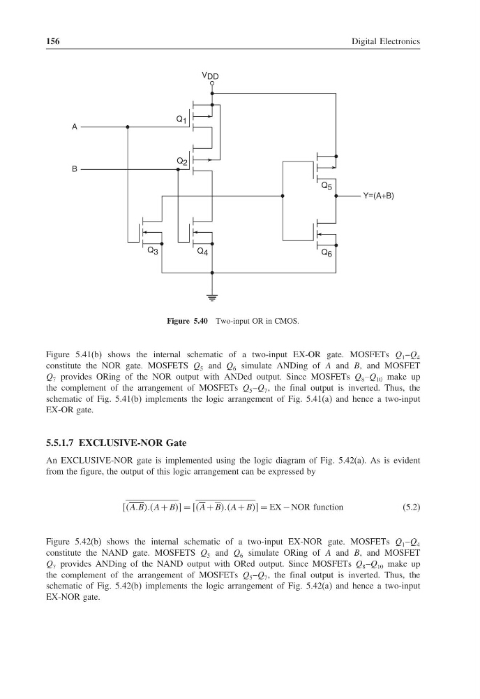
Figure 5.40 Two-input OR in CMOS.
Figure 5.41(b) shows the internal schematic of a two-input EX-OR gate. MOSFETs Q 1 –Q 4
constitute the NOR gate. MOSFETS Q 5 and Q 6 simulate ANDing of A and B, and MOSFET
Q 7 provides ORing of the NOR output with ANDed output. Since MOSFETs Q 8 –Q 10 make up
the complement of the arrangement of MOSFETs Q 5 –Q 7 , the final output is inverted. Thus, the
schematic of Fig. 5.41(b) implements the logic arrangement of Fig. 5.41(a) and hence a two-input
EX-OR gate.
5.5.1.7 EXCLUSIVE-NOR Gate
An EXCLUSIVE-NOR gate is implemented using the logic diagram of Fig. 5.42(a). As is evident
from the figure, the output of this logic arrangement can be expressed by
AABBBBA + BBB = A + BBBBA + BBB = EX − NOR function
(5.2)
Figure 5.42(b) shows the internal schematic of a two-input EX-NOR gate. MOSFETs Q 1 –Q 4
constitute the NAND gate. MOSFETS Q 5 and Q 6 simulate ORing of A and B, and MOSFET
Q 7 provides ANDing of the NAND output with ORed output. Since MOSFETs Q 8 –Q 10 make up
the complement of the arrangement of MOSFETs Q 5 –Q 7 , the final output is inverted. Thus, the
schematic of Fig. 5.42(b) implements the logic arrangement of Fig. 5.42(a) and hence a two-input
EX-NOR gate.
Digital Electronics
Y=(A+B)
V DD
A
B
Q 1
Q 2
Q 4
Q 3
Q 6
Q 5
Figure 5.40 Two-input OR in CMOS.
Figure 5.41(b) shows the internal schematic of a two-input EX-OR gate. MOSFETs Q 1 –Q 4
constitute the NOR gate. MOSFETS Q 5 and Q 6 simulate ANDing of A and B, and MOSFET
Q 7 provides ORing of the NOR output with ANDed output. Since MOSFETs Q 8 –Q 10 make up
the complement of the arrangement of MOSFETs Q 5 –Q 7 , the final output is inverted. Thus, the
schematic of Fig. 5.41(b) implements the logic arrangement of Fig. 5.41(a) and hence a two-input
EX-OR gate.
5.5.1.7 EXCLUSIVE-NOR Gate
An EXCLUSIVE-NOR gate is implemented using the logic diagram of Fig. 5.42(a). As is evident
from the figure, the output of this logic arrangement can be expressed by
AABBBBA + BBB = A + BBBBA + BBB = EX − NOR function
(5.2)
Figure 5.42(b) shows the internal schematic of a two-input EX-NOR gate. MOSFETs Q 1 –Q 4
constitute the NAND gate. MOSFETS Q 5 and Q 6 simulate ORing of A and B, and MOSFET
Q 7 provides ANDing of the NAND output with ORed output. Since MOSFETs Q 8 –Q 10 make up
the complement of the arrangement of MOSFETs Q 5 –Q 7 , the final output is inverted. Thus, the
schematic of Fig. 5.42(b) implements the logic arrangement of Fig. 5.42(a) and hence a two-input
EX-NOR gate.