

Logic Families
149
Inputs
V EE
Bias
Network
OR O/P
Q 7
V CC
Q 6
Q 5
Q 4
Q 3
Q 2
Q 1
Q 8
NOR O/P
R EE
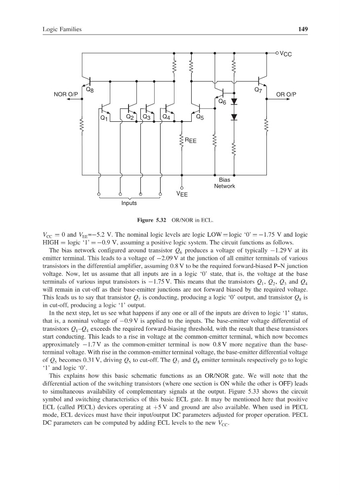
Figure 5.32 OR/NOR in ECL.
V CC = 0 and V EE =−5.2 V. The nominal logic levels are logic LOW = logic ‘0’ = −1.75 V and logic
HIGH = logic ‘1’ = −0.9 V, assuming a positive logic system. The circuit functions as follows.
The bias network configured around transistor Q 6 produces a voltage of typically −1.29 V at its
emitter terminal. This leads to a voltage of −2.09 V at the junction of all emitter terminals of various
transistors in the differential amplifier, assuming 0.8 V to be the required forward-biased P–N junction
voltage. Now, let us assume that all inputs are in a logic ‘0’ state, that is, the voltage at the base
terminals of various input transistors is −1.75 V. This means that the transistors Q 1 , Q 2 , Q 3 and Q 4
will remain in cut-off as their base-emitter junctions are not forward biased by the required voltage.
This leads us to say that transistor Q 7 is conducting, producing a logic ‘0’ output, and transistor Q 8 is
in cut-off, producing a logic ‘1’ output.
In the next step, let us see what happens if any one or all of the inputs are driven to logic ‘1’ status,
that is, a nominal voltage of −0.9 V is applied to the inputs. The base-emitter voltage differential of
transistors Q 1 –Q 4 exceeds the required forward-biasing threshold, with the result that these transistors
start conducting. This leads to a rise in voltage at the common-emitter terminal, which now becomes
approximately −1.7 V as the common-emitter terminal is now 0.8 V more negative than the baseterminal voltage. With rise in the common-emitter terminal voltage, the base-emitter differential voltage
of Q 5 becomes 0.31 V, driving Q 5 to cut-off. The Q 7 and Q 8 emitter terminals respectively go to logic
‘1’ and logic ‘0’.
This explains how this basic schematic functions as an OR/NOR gate. We will note that the
differential action of the switching transistors (where one section is ON while the other is OFF) leads
to simultaneous availability of complementary signals at the output. Figure 5.33 shows the circuit
symbol and switching characteristics of this basic ECL gate. It may be mentioned here that positive
ECL (called PECL) devices operating at +5 V and ground are also available. When used in PECL
mode, ECL devices must have their input/output DC parameters adjusted for proper operation. PECL
DC parameters can be computed by adding ECL levels to the new V CC .
149
Inputs
V EE
Bias
Network
OR O/P
Q 7
V CC
Q 6
Q 5
Q 4
Q 3
Q 2
Q 1
Q 8
NOR O/P
R EE
Figure 5.32 OR/NOR in ECL.
V CC = 0 and V EE =−5.2 V. The nominal logic levels are logic LOW = logic ‘0’ = −1.75 V and logic
HIGH = logic ‘1’ = −0.9 V, assuming a positive logic system. The circuit functions as follows.
The bias network configured around transistor Q 6 produces a voltage of typically −1.29 V at its
emitter terminal. This leads to a voltage of −2.09 V at the junction of all emitter terminals of various
transistors in the differential amplifier, assuming 0.8 V to be the required forward-biased P–N junction
voltage. Now, let us assume that all inputs are in a logic ‘0’ state, that is, the voltage at the base
terminals of various input transistors is −1.75 V. This means that the transistors Q 1 , Q 2 , Q 3 and Q 4
will remain in cut-off as their base-emitter junctions are not forward biased by the required voltage.
This leads us to say that transistor Q 7 is conducting, producing a logic ‘0’ output, and transistor Q 8 is
in cut-off, producing a logic ‘1’ output.
In the next step, let us see what happens if any one or all of the inputs are driven to logic ‘1’ status,
that is, a nominal voltage of −0.9 V is applied to the inputs. The base-emitter voltage differential of
transistors Q 1 –Q 4 exceeds the required forward-biasing threshold, with the result that these transistors
start conducting. This leads to a rise in voltage at the common-emitter terminal, which now becomes
approximately −1.7 V as the common-emitter terminal is now 0.8 V more negative than the baseterminal voltage. With rise in the common-emitter terminal voltage, the base-emitter differential voltage
of Q 5 becomes 0.31 V, driving Q 5 to cut-off. The Q 7 and Q 8 emitter terminals respectively go to logic
‘1’ and logic ‘0’.
This explains how this basic schematic functions as an OR/NOR gate. We will note that the
differential action of the switching transistors (where one section is ON while the other is OFF) leads
to simultaneous availability of complementary signals at the output. Figure 5.33 shows the circuit
symbol and switching characteristics of this basic ECL gate. It may be mentioned here that positive
ECL (called PECL) devices operating at +5 V and ground are also available. When used in PECL
mode, ECL devices must have their input/output DC parameters adjusted for proper operation. PECL
DC parameters can be computed by adding ECL levels to the new V CC .