

Logic Families
125
R 3
130
Q 3
D 1
Q 4
R 4
1K
R 2
1.6K
R 1
4K
V CC
GND
Y
Q 2
Q 1
Input A
Input B
D 2
D 3
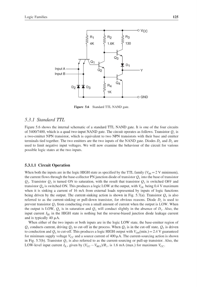
Figure 5.6 Standard TTL NAND gate.
5.3.1 Standard TTL
Figure 5.6 shows the internal schematic of a standard TTL NAND gate. It is one of the four circuits
of 5400/7400, which is a quad two-input NAND gate. The circuit operates as follows. Transistor Q 1 is
a two-emitter NPN transistor, which is equivalent to two NPN transistors with their base and emitter
terminals tied together. The two emitters are the two inputs of the NAND gate. Diodes D 2 and D 3 are
used to limit negative input voltages. We will now examine the behaviour of the circuit for various
possible logic states at the two inputs.
5.3.1.1 Circuit Operation
When both the inputs are in the logic HIGH state as specified by the TTL family (V IH = 2 V minimum),
the current flows through the base-collector PN junction diode of transistor Q 1 into the base of transistor
Q 2 . Transistor Q 2 is turned ON to saturation, with the result that transistor Q 3 is switched OFF and
transistor Q 4 is switched ON. This produces a logic LOW at the output, with V OL being 0.4 V maximum
when it is sinking a current of 16 mA from external loads represented by inputs of logic functions
being driven by the output. The current-sinking action is shown in Fig. 5.7(a). Transistor Q 4 is also
referred to as the current-sinking or pull-down transistor, for obvious reasons. Diode D 1 is used to
prevent transistor Q 3 from conducting even a small amount of current when the output is LOW. When
the output is LOW, Q 4 is in saturation and Q 3 will conduct slightly in the absence of D 1 . Also, the
input current I IH in the HIGH state is nothing but the reverse-biased junction diode leakage current
and is typically 40 A.
When either of the two inputs or both inputs are in the logic LOW state, the base-emitter region of
Q 1 conducts current, driving Q 2 to cut-off in the process. When Q 2 is in the cut-off state, Q 3 is driven
to conduction and Q 4 to cut-off. This produces a logic HIGH output with V OH (min.) = 2.4 V guaranteed
for minimum supply voltage V CC and a source current of 400 A. The current-sourcing action is shown
in Fig. 5.7(b). Transistor Q 3 is also referred to as the current-sourcing or pull-up transistor. Also, the
LOW-level input current I IL , given by (V CC − V BE1 /R 1 , is 1.6 mA (max.) for maximum V CC .
125
R 3
130
Q 3
D 1
Q 4
R 4
1K
R 2
1.6K
R 1
4K
V CC
GND
Y
Q 2
Q 1
Input A
Input B
D 2
D 3
Figure 5.6 Standard TTL NAND gate.
5.3.1 Standard TTL
Figure 5.6 shows the internal schematic of a standard TTL NAND gate. It is one of the four circuits
of 5400/7400, which is a quad two-input NAND gate. The circuit operates as follows. Transistor Q 1 is
a two-emitter NPN transistor, which is equivalent to two NPN transistors with their base and emitter
terminals tied together. The two emitters are the two inputs of the NAND gate. Diodes D 2 and D 3 are
used to limit negative input voltages. We will now examine the behaviour of the circuit for various
possible logic states at the two inputs.
5.3.1.1 Circuit Operation
When both the inputs are in the logic HIGH state as specified by the TTL family (V IH = 2 V minimum),
the current flows through the base-collector PN junction diode of transistor Q 1 into the base of transistor
Q 2 . Transistor Q 2 is turned ON to saturation, with the result that transistor Q 3 is switched OFF and
transistor Q 4 is switched ON. This produces a logic LOW at the output, with V OL being 0.4 V maximum
when it is sinking a current of 16 mA from external loads represented by inputs of logic functions
being driven by the output. The current-sinking action is shown in Fig. 5.7(a). Transistor Q 4 is also
referred to as the current-sinking or pull-down transistor, for obvious reasons. Diode D 1 is used to
prevent transistor Q 3 from conducting even a small amount of current when the output is LOW. When
the output is LOW, Q 4 is in saturation and Q 3 will conduct slightly in the absence of D 1 . Also, the
input current I IH in the HIGH state is nothing but the reverse-biased junction diode leakage current
and is typically 40 A.
When either of the two inputs or both inputs are in the logic LOW state, the base-emitter region of
Q 1 conducts current, driving Q 2 to cut-off in the process. When Q 2 is in the cut-off state, Q 3 is driven
to conduction and Q 4 to cut-off. This produces a logic HIGH output with V OH (min.) = 2.4 V guaranteed
for minimum supply voltage V CC and a source current of 400 A. The current-sourcing action is shown
in Fig. 5.7(b). Transistor Q 3 is also referred to as the current-sourcing or pull-up transistor. Also, the
LOW-level input current I IL , given by (V CC − V BE1 /R 1 , is 1.6 mA (max.) for maximum V CC .