

96
Digital Electronics
I IH
I IH
I IH
I OH
(a)
I IL
I IL
I IL
I OL
(b)
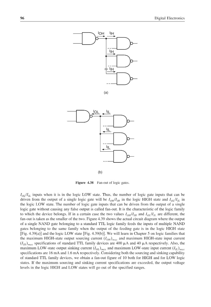
Figure 4.38 Fan-out of logic gates.
I OL /I IL inputs when it is in the logic LOW state. Thus, the number of logic gate inputs that can be
driven from the output of a single logic gate will be I OH /I IH in the logic HIGH state and I OL /I IL in
the logic LOW state. The number of logic gate inputs that can be driven from the output of a single
logic gate without causing any false output is called fan-out. It is the characteristic of the logic family
to which the device belongs. If in a certain case the two values I OH /I IH and I OL /I IL are different, the
fan-out is taken as the smaller of the two. Figure 4.39 shows the actual circuit diagram where the output
of a single NAND gate belonging to a standard TTL logic family feeds the inputs of multiple NAND
gates belonging to the same family when the output of the feeding gate is in the logic HIGH state
[Fig. 4.39(a)] and the logic LOW state [Fig. 4.39(b)]. We will learn in Chapter 5 on logic families that
the maximum HIGH-state output sourcing current (I OH max and maximum HIGH-state input current
(I IH max specifications of standard TTL family devices are 400 A and 40 A respectively. Also, the
maximum LOW-state output sinking current (I OL max and maximum LOW-state input current (I IL max
specifications are 16 mA and 1.6 mA respectively. Considering both the sourcing and sinking capability
of standard TTL family devices, we obtain a fan-out figure of 10 both for HIGH and for LOW logic
states. If the maximum sourcing and sinking current specifications are exceeded, the output voltage
levels in the logic HIGH and LOW states will go out of the specified ranges.
Digital Electronics
I IH
I IH
I IH
I OH
(a)
I IL
I IL
I IL
I OL
(b)
Figure 4.38 Fan-out of logic gates.
I OL /I IL inputs when it is in the logic LOW state. Thus, the number of logic gate inputs that can be
driven from the output of a single logic gate will be I OH /I IH in the logic HIGH state and I OL /I IL in
the logic LOW state. The number of logic gate inputs that can be driven from the output of a single
logic gate without causing any false output is called fan-out. It is the characteristic of the logic family
to which the device belongs. If in a certain case the two values I OH /I IH and I OL /I IL are different, the
fan-out is taken as the smaller of the two. Figure 4.39 shows the actual circuit diagram where the output
of a single NAND gate belonging to a standard TTL logic family feeds the inputs of multiple NAND
gates belonging to the same family when the output of the feeding gate is in the logic HIGH state
[Fig. 4.39(a)] and the logic LOW state [Fig. 4.39(b)]. We will learn in Chapter 5 on logic families that
the maximum HIGH-state output sourcing current (I OH max and maximum HIGH-state input current
(I IH max specifications of standard TTL family devices are 400 A and 40 A respectively. Also, the
maximum LOW-state output sinking current (I OL max and maximum LOW-state input current (I IL max
specifications are 16 mA and 1.6 mA respectively. Considering both the sourcing and sinking capability
of standard TTL family devices, we obtain a fan-out figure of 10 both for HIGH and for LOW logic
states. If the maximum sourcing and sinking current specifications are exceeded, the output voltage
levels in the logic HIGH and LOW states will go out of the specified ranges.