

Logic Gates and Related Devices
95
A
B
C
D
+V
Y
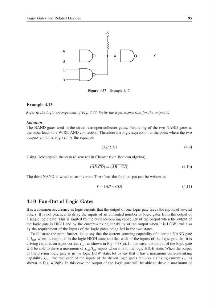
Figure 4.37 Example 4.13.
Example 4.13
Refer to the logic arrangement of Fig. 4.37. Write the logic expression for the output Y.
Solution
The NAND gates used in the circuit are open collector gates. Paralleling of the two NAND gates at
the input leads to a WIRE-AND connection. Therefore the logic expression at the point where the two
outputs combine is given by the equation
ABBCDD
(4.9)
Using DeMorgan’s theorem (discussed in Chapter 6 on Boolean algebra),
ABBCDD = AB + CDD
(4.10)
The third NAND is wired as an inverter. Therefore, the final output can be written as
Y = AB + CDD
(4.11)
4.10 Fan-Out of Logic Gates
It is a common occurrence in logic circuits that the output of one logic gate feeds the inputs of several
others. It is not practical to drive the inputs of an unlimited number of logic gates from the output of
a single logic gate. This is limited by the current-sourcing capability of the output when the output of
the logic gate is HIGH and by the current-sinking capability of the output when it is LOW, and also
by the requirement of the inputs of the logic gates being fed in the two states.
To illustrate the point further, let us say that the current-sourcing capability of a certain NAND gate
is I OH when its output is in the logic HIGH state and that each of the inputs of the logic gate that it is
driving requires an input current I IH , as shown in Fig. 4.38(a). In this case, the output of the logic gate
will be able to drive a maximum of I OH /I IH inputs when it is in the logic HIGH state. When the output
of the driving logic gate is in the logic LOW state, let us say that it has a maximum current-sinking
capability I OL , and that each of the inputs of the driven logic gates requires a sinking current I IL , as
shown in Fig. 4.38(b). In this case the output of the logic gate will be able to drive a maximum of
95
A
B
C
D
+V
Y
Figure 4.37 Example 4.13.
Example 4.13
Refer to the logic arrangement of Fig. 4.37. Write the logic expression for the output Y.
Solution
The NAND gates used in the circuit are open collector gates. Paralleling of the two NAND gates at
the input leads to a WIRE-AND connection. Therefore the logic expression at the point where the two
outputs combine is given by the equation
ABBCDD
(4.9)
Using DeMorgan’s theorem (discussed in Chapter 6 on Boolean algebra),
ABBCDD = AB + CDD
(4.10)
The third NAND is wired as an inverter. Therefore, the final output can be written as
Y = AB + CDD
(4.11)
4.10 Fan-Out of Logic Gates
It is a common occurrence in logic circuits that the output of one logic gate feeds the inputs of several
others. It is not practical to drive the inputs of an unlimited number of logic gates from the output of
a single logic gate. This is limited by the current-sourcing capability of the output when the output of
the logic gate is HIGH and by the current-sinking capability of the output when it is LOW, and also
by the requirement of the inputs of the logic gates being fed in the two states.
To illustrate the point further, let us say that the current-sourcing capability of a certain NAND gate
is I OH when its output is in the logic HIGH state and that each of the inputs of the logic gate that it is
driving requires an input current I IH , as shown in Fig. 4.38(a). In this case, the output of the logic gate
will be able to drive a maximum of I OH /I IH inputs when it is in the logic HIGH state. When the output
of the driving logic gate is in the logic LOW state, let us say that it has a maximum current-sinking
capability I OL , and that each of the inputs of the driven logic gates requires a sinking current I IL , as
shown in Fig. 4.38(b). In this case the output of the logic gate will be able to drive a maximum of