

86
Digital Electronics
A
(a)
Y=A
A
B
Y=A+B
(b)
B
A
(c)
Y=A.B
A
B
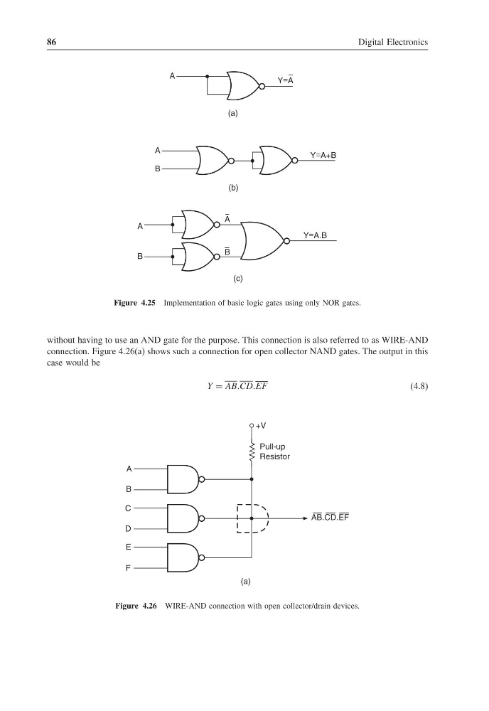
Figure 4.25 Implementation of basic logic gates using only NOR gates.
without having to use an AND gate for the purpose. This connection is also referred to as WIRE-AND
connection. Figure 4.26(a) shows such a connection for open collector NAND gates. The output in this
case would be
Y = ABBCDDEF
(4.8)
A
B
C
D
E
F
+V
Pull-up
Resistor
AB.CD.EF
(a)
Figure 4.26 WIRE-AND connection with open collector/drain devices.
Digital Electronics
A
(a)
Y=A
A
B
Y=A+B
(b)
B
A
(c)
Y=A.B
A
B
Figure 4.25 Implementation of basic logic gates using only NOR gates.
without having to use an AND gate for the purpose. This connection is also referred to as WIRE-AND
connection. Figure 4.26(a) shows such a connection for open collector NAND gates. The output in this
case would be
Y = ABBCDDEF
(4.8)
A
B
C
D
E
F
+V
Pull-up
Resistor
AB.CD.EF
(a)
Figure 4.26 WIRE-AND connection with open collector/drain devices.