

Logic Gates and Related Devices
79
4.3.5 NAND Gate
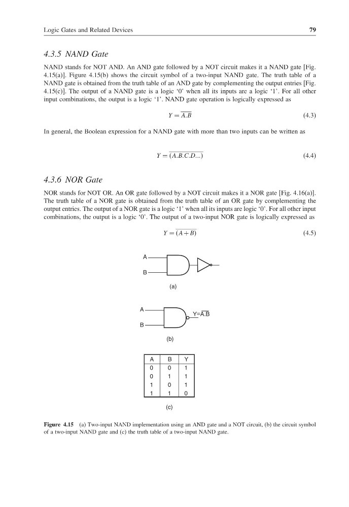
NAND stands for NOT AND. An AND gate followed by a NOT circuit makes it a NAND gate [Fig.
4.15(a)]. Figure 4.15(b) shows the circuit symbol of a two-input NAND gate. The truth table of a
NAND gate is obtained from the truth table of an AND gate by complementing the output entries [Fig.
4.15(c)]. The output of a NAND gate is a logic ‘0’ when all its inputs are a logic ‘1’. For all other
input combinations, the output is a logic ‘1’. NAND gate operation is logically expressed as
Y = AAB
(4.3)
In general, the Boolean expression for a NAND gate with more than two inputs can be written as
Y = AABBCCDDDDD
(4.4)
4.3.6 NOR Gate
NOR stands for NOT OR. An OR gate followed by a NOT circuit makes it a NOR gate [Fig. 4.16(a)].
The truth table of a NOR gate is obtained from the truth table of an OR gate by complementing the
output entries. The output of a NOR gate is a logic ‘1’ when all its inputs are logic ‘0’. For all other input
combinations, the output is a logic ‘0’. The output of a two-input NOR gate is logically expressed as
Y = A + BB
(4.5)
A
0
0
1
1
B
0
1
0
1
Y
1
1
1
0
(c)
A
B
(a)
A
B
(b)
Y=A.B
Figure 4.15 (a) Two-input NAND implementation using an AND gate and a NOT circuit, (b) the circuit symbol
of a two-input NAND gate and (c) the truth table of a two-input NAND gate.
79
4.3.5 NAND Gate
NAND stands for NOT AND. An AND gate followed by a NOT circuit makes it a NAND gate [Fig.
4.15(a)]. Figure 4.15(b) shows the circuit symbol of a two-input NAND gate. The truth table of a
NAND gate is obtained from the truth table of an AND gate by complementing the output entries [Fig.
4.15(c)]. The output of a NAND gate is a logic ‘0’ when all its inputs are a logic ‘1’. For all other
input combinations, the output is a logic ‘1’. NAND gate operation is logically expressed as
Y = AAB
(4.3)
In general, the Boolean expression for a NAND gate with more than two inputs can be written as
Y = AABBCCDDDDD
(4.4)
4.3.6 NOR Gate
NOR stands for NOT OR. An OR gate followed by a NOT circuit makes it a NOR gate [Fig. 4.16(a)].
The truth table of a NOR gate is obtained from the truth table of an OR gate by complementing the
output entries. The output of a NOR gate is a logic ‘1’ when all its inputs are logic ‘0’. For all other input
combinations, the output is a logic ‘0’. The output of a two-input NOR gate is logically expressed as
Y = A + BB
(4.5)
A
0
0
1
1
B
0
1
0
1
Y
1
1
1
0
(c)
A
B
(a)
A
B
(b)
Y=A.B
Figure 4.15 (a) Two-input NAND implementation using an AND gate and a NOT circuit, (b) the circuit symbol
of a two-input NAND gate and (c) the truth table of a two-input NAND gate.