

4.1 Nanoscience
159
μ R
0
μ L
ε
Current I sd
Quantum dot
V sd
Drain
Source
Electron flow
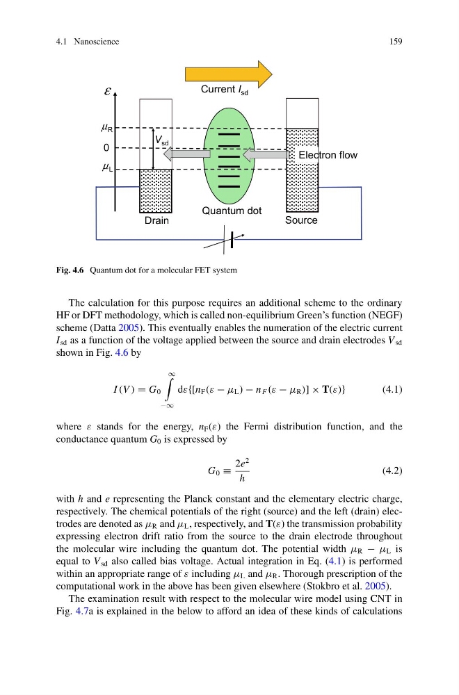
Fig. 4.6 Quantum dot for a molecular FET system
The calculation for this purpose requires an additional scheme to the ordinary
HF or DFT methodology, which is called non-equilibrium Green’s function (NEGF)
scheme (Datta 2005). This eventually enables the numeration of the electric current
I sd as a function of the voltage applied between the source and drain electrodes V sd
shown in Fig. 4.6 by
I (V ) = G 0
∞
−∞
dε{[n F (ε − μ L ) − n F (ε − μ R )] × T(ε)}
(4.1)
where ε stands for the energy, n F (ε) the Fermi distribution function, and the
conductance quantum G 0 is expressed by
G 0 ≡
2e
2
h
(4.2)
with h and e representing the Planck constant and the elementary electric charge,
respectively. The chemical potentials of the right (source) and the left (drain) electrodes are denoted as μ R and μ L , respectively, and T(ε) the transmission probability
expressing electron drift ratio from the source to the drain electrode throughout
the molecular wire including the quantum dot. The potential width μ R − μ L is
equal to V sd also called bias voltage. Actual integration in Eq. (4.1) is performed
within an appropriate range of ε including μ L and μ R . Thorough prescription of the
computational work in the above has been given elsewhere (Stokbro et al. 2005).
The examination result with respect to the molecular wire model using CNT in
Fig. 4.7a is explained in the below to afford an idea of these kinds of calculations
159
μ R
0
μ L
ε
Current I sd
Quantum dot
V sd
Drain
Source
Electron flow
Fig. 4.6 Quantum dot for a molecular FET system
The calculation for this purpose requires an additional scheme to the ordinary
HF or DFT methodology, which is called non-equilibrium Green’s function (NEGF)
scheme (Datta 2005). This eventually enables the numeration of the electric current
I sd as a function of the voltage applied between the source and drain electrodes V sd
shown in Fig. 4.6 by
I (V ) = G 0
∞
−∞
dε{[n F (ε − μ L ) − n F (ε − μ R )] × T(ε)}
(4.1)
where ε stands for the energy, n F (ε) the Fermi distribution function, and the
conductance quantum G 0 is expressed by
G 0 ≡
2e
2
h
(4.2)
with h and e representing the Planck constant and the elementary electric charge,
respectively. The chemical potentials of the right (source) and the left (drain) electrodes are denoted as μ R and μ L , respectively, and T(ε) the transmission probability
expressing electron drift ratio from the source to the drain electrode throughout
the molecular wire including the quantum dot. The potential width μ R − μ L is
equal to V sd also called bias voltage. Actual integration in Eq. (4.1) is performed
within an appropriate range of ε including μ L and μ R . Thorough prescription of the
computational work in the above has been given elsewhere (Stokbro et al. 2005).
The examination result with respect to the molecular wire model using CNT in
Fig. 4.7a is explained in the below to afford an idea of these kinds of calculations