

422
N. Shimoi
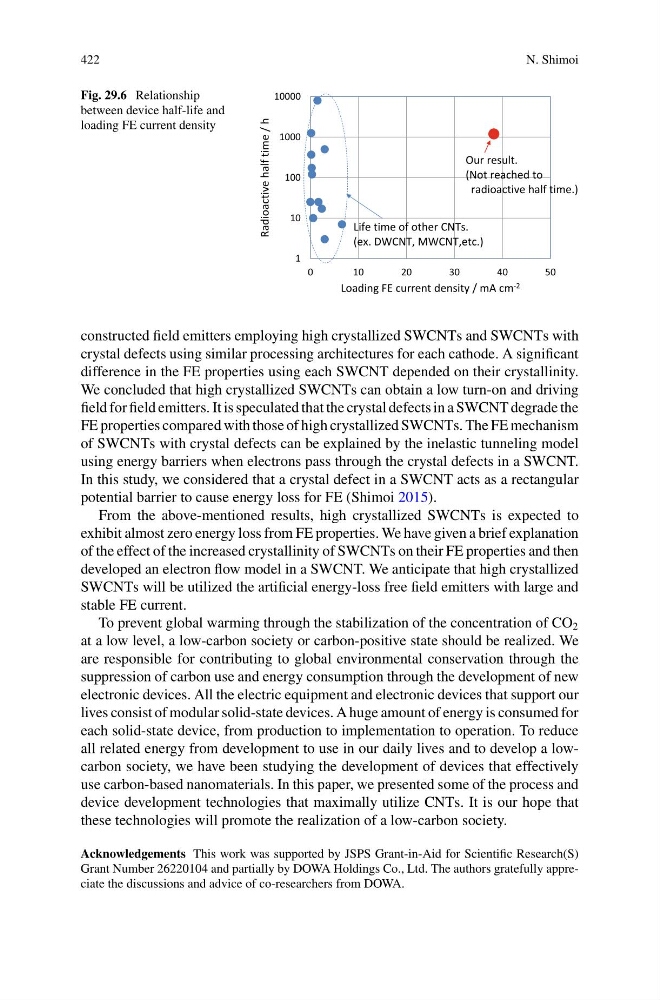
Fig. 29.6 Relationship
between device half-life and
loading FE current density
1
10
100
1000
10000
0
1 0
2 0
3 0
4 0
5 0
Radioactive half time / h
Loading FE current density / mA cm -2
Our result.
(Not reached to
radioactive half time.)
Life time of other CNTs.
(ex. DWCNT, MWCNT,etc.)
constructed field emitters employing high crystallized SWCNTs and SWCNTs with
crystal defects using similar processing architectures for each cathode. A significant
difference in the FE properties using each SWCNT depended on their crystallinity.
We concluded that high crystallized SWCNTs can obtain a low turn-on and driving
field for field emitters. It is speculated that the crystal defects in a SWCNT degrade the
FE properties compared with those of high crystallized SWCNTs. The FE mechanism
of SWCNTs with crystal defects can be explained by the inelastic tunneling model
using energy barriers when electrons pass through the crystal defects in a SWCNT.
In this study, we considered that a crystal defect in a SWCNT acts as a rectangular
potential barrier to cause energy loss for FE (Shimoi 2015).
From the above-mentioned results, high crystallized SWCNTs is expected to
exhibit almost zero energy loss from FE properties. We have given a brief explanation
of the effect of the increased crystallinity of SWCNTs on their FE properties and then
developed an electron flow model in a SWCNT. We anticipate that high crystallized
SWCNTs will be utilized the artificial energy-loss free field emitters with large and
stable FE current.
To prevent global warming through the stabilization of the concentration of CO 2
at a low level, a low-carbon society or carbon-positive state should be realized. We
are responsible for contributing to global environmental conservation through the
suppression of carbon use and energy consumption through the development of new
electronic devices. All the electric equipment and electronic devices that support our
lives consist of modular solid-state devices. A huge amount of energy is consumed for
each solid-state device, from production to implementation to operation. To reduce
all related energy from development to use in our daily lives and to develop a lowcarbon society, we have been studying the development of devices that effectively
use carbon-based nanomaterials. In this paper, we presented some of the process and
device development technologies that maximally utilize CNTs. It is our hope that
these technologies will promote the realization of a low-carbon society.
Acknowledgements This work was supported by JSPS Grant-in-Aid for Scientific Research(S)
Grant Number 26220104 and partially by DOWA Holdings Co., Ltd. The authors gratefully appreciate the discussions and advice of co-researchers from DOWA.
N. Shimoi
Fig. 29.6 Relationship
between device half-life and
loading FE current density
1
10
100
1000
10000
0
1 0
2 0
3 0
4 0
5 0
Radioactive half time / h
Loading FE current density / mA cm -2
Our result.
(Not reached to
radioactive half time.)
Life time of other CNTs.
(ex. DWCNT, MWCNT,etc.)
constructed field emitters employing high crystallized SWCNTs and SWCNTs with
crystal defects using similar processing architectures for each cathode. A significant
difference in the FE properties using each SWCNT depended on their crystallinity.
We concluded that high crystallized SWCNTs can obtain a low turn-on and driving
field for field emitters. It is speculated that the crystal defects in a SWCNT degrade the
FE properties compared with those of high crystallized SWCNTs. The FE mechanism
of SWCNTs with crystal defects can be explained by the inelastic tunneling model
using energy barriers when electrons pass through the crystal defects in a SWCNT.
In this study, we considered that a crystal defect in a SWCNT acts as a rectangular
potential barrier to cause energy loss for FE (Shimoi 2015).
From the above-mentioned results, high crystallized SWCNTs is expected to
exhibit almost zero energy loss from FE properties. We have given a brief explanation
of the effect of the increased crystallinity of SWCNTs on their FE properties and then
developed an electron flow model in a SWCNT. We anticipate that high crystallized
SWCNTs will be utilized the artificial energy-loss free field emitters with large and
stable FE current.
To prevent global warming through the stabilization of the concentration of CO 2
at a low level, a low-carbon society or carbon-positive state should be realized. We
are responsible for contributing to global environmental conservation through the
suppression of carbon use and energy consumption through the development of new
electronic devices. All the electric equipment and electronic devices that support our
lives consist of modular solid-state devices. A huge amount of energy is consumed for
each solid-state device, from production to implementation to operation. To reduce
all related energy from development to use in our daily lives and to develop a lowcarbon society, we have been studying the development of devices that effectively
use carbon-based nanomaterials. In this paper, we presented some of the process and
device development technologies that maximally utilize CNTs. It is our hope that
these technologies will promote the realization of a low-carbon society.
Acknowledgements This work was supported by JSPS Grant-in-Aid for Scientific Research(S)
Grant Number 26220104 and partially by DOWA Holdings Co., Ltd. The authors gratefully appreciate the discussions and advice of co-researchers from DOWA.