

418
N. Shimoi
1.0E-06
1.0E-05
1.0E-04
1.0E-03
0.5
1
1.5
2
2.5
3
Current density / A cm -2
Electrical field / V µm -1
Highly crystalline
SWCNTs
Un-annealed
SWCNTs
(a)
High - brightness spot
Low - brightness
spot
Highly crystalline SWCNTs
250 µA/cm 2 @E=1.3V/µm
20 µm
High - brightness spot
Low- brightness spot
Un-annealed SWCNTs
250 µA/cm 2 @E=2.5V/µm
20 µm
(b) Initial plannar lighting homogeneity
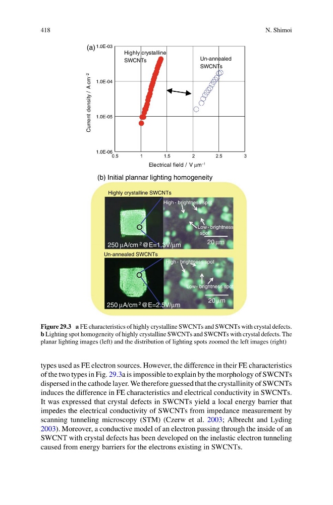
Figure 29.3 a FE characteristics of highly crystalline SWCNTs and SWCNTs with crystal defects.
b Lighting spot homogeneity of highly crystalline SWCNTs and SWCNTs with crystal defects. The
planar lighting images (left) and the distribution of lighting spots zoomed the left images (right)
types used as FE electron sources. However, the difference in their FE characteristics
of the two types in Fig. 29.3a is impossible to explain by the morphology of SWCNTs
dispersed in the cathode layer. We therefore guessed that the crystallinity of SWCNTs
induces the difference in FE characteristics and electrical conductivity in SWCNTs.
It was expressed that crystal defects in SWCNTs yield a local energy barrier that
impedes the electrical conductivity of SWCNTs from impedance measurement by
scanning tunneling microscopy (STM) (Czerw et al. 2003; Albrecht and Lyding
2003). Moreover, a conductive model of an electron passing through the inside of an
SWCNT with crystal defects has been developed on the inelastic electron tunneling
caused from energy barriers for the electrons existing in SWCNTs.
N. Shimoi
1.0E-06
1.0E-05
1.0E-04
1.0E-03
0.5
1
1.5
2
2.5
3
Current density / A cm -2
Electrical field / V µm -1
Highly crystalline
SWCNTs
Un-annealed
SWCNTs
(a)
High - brightness spot
Low - brightness
spot
Highly crystalline SWCNTs
250 µA/cm 2 @E=1.3V/µm
20 µm
High - brightness spot
Low- brightness spot
Un-annealed SWCNTs
250 µA/cm 2 @E=2.5V/µm
20 µm
(b) Initial plannar lighting homogeneity
Figure 29.3 a FE characteristics of highly crystalline SWCNTs and SWCNTs with crystal defects.
b Lighting spot homogeneity of highly crystalline SWCNTs and SWCNTs with crystal defects. The
planar lighting images (left) and the distribution of lighting spots zoomed the left images (right)
types used as FE electron sources. However, the difference in their FE characteristics
of the two types in Fig. 29.3a is impossible to explain by the morphology of SWCNTs
dispersed in the cathode layer. We therefore guessed that the crystallinity of SWCNTs
induces the difference in FE characteristics and electrical conductivity in SWCNTs.
It was expressed that crystal defects in SWCNTs yield a local energy barrier that
impedes the electrical conductivity of SWCNTs from impedance measurement by
scanning tunneling microscopy (STM) (Czerw et al. 2003; Albrecht and Lyding
2003). Moreover, a conductive model of an electron passing through the inside of an
SWCNT with crystal defects has been developed on the inelastic electron tunneling
caused from energy barriers for the electrons existing in SWCNTs.