

when it is absorbed by the sensing material. In
some cases, this can be achieved more easily by
adding a specific catalyst to the material, since
catalysts modify the band gap; gases with an ionization energy resembling the band gap are preferentially adsorbed. The band gap of the sensing
material determines which compounds the sensor
can detect: the larger the bandgap of the sensing
material, the larger molecules the sensor is capable
of detecting and vice versa, see Table 3 and Fig. 7.
Temperature Cycling
Many properties of a semiconductor sensor depend
on temperature. These include the rates of gas
adsorption and desorption, the rate of decomposition of reducing gases, and the charge-carrier diffusion length. Furthermore, many of the reactions that
take place on the surface of the sensor are exothermic which can change the temperature of the sensor.
Because the sensors themselves and the surface
chemical processes are temperature dependent, the
relationship is complex. Different gases have different characteristic conductance-temperature profiles.
Temperature cycling is a method whereby the temperature dependence of the signal is probed repeatedly and analyzed to extract useful information, in
particular regarding gas concentrations but also sensor status. This method can improve performance
and in some cases reduce cross-sensitivity
[69]. Temperature modulation has several advantages; it can give a specific signature for each gas
present, and cycles to higher temperatures can be
used to clean the surface. In addition, the information gathered from modulation can give improved
sensitivity. There is likely to be a maximum in
sensitivity linked to the shape of the conductance
versus temperature curve [55].
One study examined sensor performance for
quasi-continuous temperature cycling. In this
study, the temperature cycle consisted of two
10 s excursions from room temperature to
400
C and back to room temperature. The path
down to room temperature was performed over
50 steps, each with a duration of 200 ms. There
was no heating during the remaining part of the
cycle.
n-type semiconductor
p-type semiconductor
Electron
depletion layer
Hole
accumulation
layer
target gas
e
–
e –
e
–
e
–
target gas
receptor
transducer
utility
transducer
h
+
utility
receptor
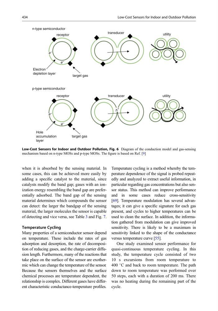
Low-Cost Sensors for Indoor and Outdoor Pollution, Fig. 6 Diagram of the conduction model and gas-sensing
mechanism based on n-type MOSs and p-type MOSs. The figure is based on Ref. [9]
434
Low-Cost Sensors for Indoor and Outdoor Pollution
some cases, this can be achieved more easily by
adding a specific catalyst to the material, since
catalysts modify the band gap; gases with an ionization energy resembling the band gap are preferentially adsorbed. The band gap of the sensing
material determines which compounds the sensor
can detect: the larger the bandgap of the sensing
material, the larger molecules the sensor is capable
of detecting and vice versa, see Table 3 and Fig. 7.
Temperature Cycling
Many properties of a semiconductor sensor depend
on temperature. These include the rates of gas
adsorption and desorption, the rate of decomposition of reducing gases, and the charge-carrier diffusion length. Furthermore, many of the reactions that
take place on the surface of the sensor are exothermic which can change the temperature of the sensor.
Because the sensors themselves and the surface
chemical processes are temperature dependent, the
relationship is complex. Different gases have different characteristic conductance-temperature profiles.
Temperature cycling is a method whereby the temperature dependence of the signal is probed repeatedly and analyzed to extract useful information, in
particular regarding gas concentrations but also sensor status. This method can improve performance
and in some cases reduce cross-sensitivity
[69]. Temperature modulation has several advantages; it can give a specific signature for each gas
present, and cycles to higher temperatures can be
used to clean the surface. In addition, the information gathered from modulation can give improved
sensitivity. There is likely to be a maximum in
sensitivity linked to the shape of the conductance
versus temperature curve [55].
One study examined sensor performance for
quasi-continuous temperature cycling. In this
study, the temperature cycle consisted of two
10 s excursions from room temperature to
400
C and back to room temperature. The path
down to room temperature was performed over
50 steps, each with a duration of 200 ms. There
was no heating during the remaining part of the
cycle.
n-type semiconductor
p-type semiconductor
Electron
depletion layer
Hole
accumulation
layer
target gas
e
–
e –
e
–
e
–
target gas
receptor
transducer
utility
transducer
h
+
utility
receptor
Low-Cost Sensors for Indoor and Outdoor Pollution, Fig. 6 Diagram of the conduction model and gas-sensing
mechanism based on n-type MOSs and p-type MOSs. The figure is based on Ref. [9]
434
Low-Cost Sensors for Indoor and Outdoor Pollution