

4.2 Particulate Silica Dispersion as Revealed by 3D-TEM
67
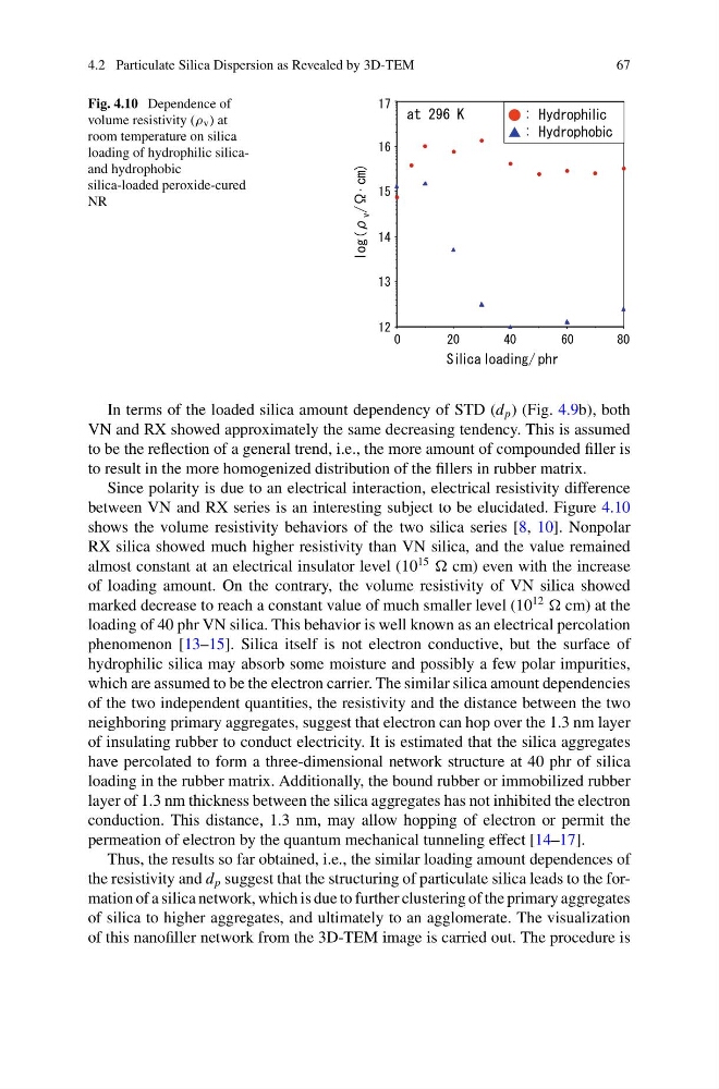
Fig. 4.10 Dependence of
volume resistivity (ρ v ) at
room temperature on silica
loading of hydrophilic silicaand hydrophobic
silica-loaded peroxide-cured
NR
In terms of the loaded silica amount dependency of STD (d p ) (Fig. 4.9b), both
VN and RX showed approximately the same decreasing tendency. This is assumed
to be the reflection of a general trend, i.e., the more amount of compounded filler is
to result in the more homogenized distribution of the fillers in rubber matrix.
Since polarity is due to an electrical interaction, electrical resistivity difference
between VN and RX series is an interesting subject to be elucidated. Figure 4.10
shows the volume resistivity behaviors of the two silica series [8, 10]. Nonpolar
RX silica showed much higher resistivity than VN silica, and the value remained
almost constant at an electrical insulator level (10
15
cm) even with the increase
of loading amount. On the contrary, the volume resistivity of VN silica showed
marked decrease to reach a constant value of much smaller level (10
12
cm) at the
loading of 40 phr VN silica. This behavior is well known as an electrical percolation
phenomenon [13–15]. Silica itself is not electron conductive, but the surface of
hydrophilic silica may absorb some moisture and possibly a few polar impurities,
which are assumed to be the electron carrier. The similar silica amount dependencies
of the two independent quantities, the resistivity and the distance between the two
neighboring primary aggregates, suggest that electron can hop over the 1.3 nm layer
of insulating rubber to conduct electricity. It is estimated that the silica aggregates
have percolated to form a three-dimensional network structure at 40 phr of silica
loading in the rubber matrix. Additionally, the bound rubber or immobilized rubber
layer of 1.3 nm thickness between the silica aggregates has not inhibited the electron
conduction. This distance, 1.3 nm, may allow hopping of electron or permit the
permeation of electron by the quantum mechanical tunneling effect [14–17].
Thus, the results so far obtained, i.e., the similar loading amount dependences of
the resistivity and d p suggest that the structuring of particulate silica leads to the formation of a silica network, which is due to further clustering of the primary aggregates
of silica to higher aggregates, and ultimately to an agglomerate. The visualization
of this nanofiller network from the 3D-TEM image is carried out. The procedure is
67
Fig. 4.10 Dependence of
volume resistivity (ρ v ) at
room temperature on silica
loading of hydrophilic silicaand hydrophobic
silica-loaded peroxide-cured
NR
In terms of the loaded silica amount dependency of STD (d p ) (Fig. 4.9b), both
VN and RX showed approximately the same decreasing tendency. This is assumed
to be the reflection of a general trend, i.e., the more amount of compounded filler is
to result in the more homogenized distribution of the fillers in rubber matrix.
Since polarity is due to an electrical interaction, electrical resistivity difference
between VN and RX series is an interesting subject to be elucidated. Figure 4.10
shows the volume resistivity behaviors of the two silica series [8, 10]. Nonpolar
RX silica showed much higher resistivity than VN silica, and the value remained
almost constant at an electrical insulator level (10
15
cm) even with the increase
of loading amount. On the contrary, the volume resistivity of VN silica showed
marked decrease to reach a constant value of much smaller level (10
12
cm) at the
loading of 40 phr VN silica. This behavior is well known as an electrical percolation
phenomenon [13–15]. Silica itself is not electron conductive, but the surface of
hydrophilic silica may absorb some moisture and possibly a few polar impurities,
which are assumed to be the electron carrier. The similar silica amount dependencies
of the two independent quantities, the resistivity and the distance between the two
neighboring primary aggregates, suggest that electron can hop over the 1.3 nm layer
of insulating rubber to conduct electricity. It is estimated that the silica aggregates
have percolated to form a three-dimensional network structure at 40 phr of silica
loading in the rubber matrix. Additionally, the bound rubber or immobilized rubber
layer of 1.3 nm thickness between the silica aggregates has not inhibited the electron
conduction. This distance, 1.3 nm, may allow hopping of electron or permit the
permeation of electron by the quantum mechanical tunneling effect [14–17].
Thus, the results so far obtained, i.e., the similar loading amount dependences of
the resistivity and d p suggest that the structuring of particulate silica leads to the formation of a silica network, which is due to further clustering of the primary aggregates
of silica to higher aggregates, and ultimately to an agglomerate. The visualization
of this nanofiller network from the 3D-TEM image is carried out. The procedure is