

• Appropriate band-gap energy in the range of 1.7–3.2 eV
• Efficient light absorption
• High carrier mobility
• Precise band edge positions that straddle the water redox potentials
• Lack of toxicity and chemical stability (Boudjemaa et al. 2013; Zazoua et al.
2014; Helaili et al. 2015)
In heterogeneous photocatalysis, when photons of energy higher or equal to the
band-gap energy are absorbed by a semiconductor, an electron (e
À
) from the valence
band (VB) is transferred to the conduction band (CB) generating a hole (h
+
) in the
VB. Thus, the absorption of photons creates electron/hole pairs (e
À /h
+
) which can
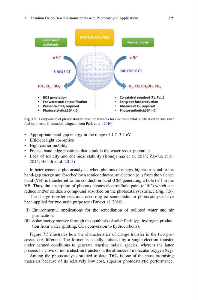
reduce and/or oxidize a compound adsorbed on the photocatalyst surface (Fig. 7.5).
The charge transfer reactions occurring on semiconductor photocatalysts have
been applied for two main purposes: (Park et al. 2016)
(i) Environmental applications for the remediation of polluted water and air
purification.
(ii) Solar energy storage through the synthesis of solar fuels (eg. hydrogen production from water splitting, CO 2 conversion to hydrocarbons).
Figure 7.5 illustrates how the characteristics of charge transfer in the two processes are different. The former is usually initiated by a single-electron transfer
under aerated conditions to generate reactive radical species, whereas the latter
proceeds via two or more electron transfers in the absence of molecular oxygen (O 2 ).
Among the photocatalysts studied to date, TiO 2 is one of the most promising
materials because of its relatively low cost, superior photocatalytic performance,
Fig. 7.5 Comparison of photocatalytic reaction features for environmental purification versus solar
fuel synthesis. Illustration adapted from Park et al. (2016)
7 Titanium Oxide-Based Nanomaterials with Photocatalytic Applications. . .
225
• Efficient light absorption
• High carrier mobility
• Precise band edge positions that straddle the water redox potentials
• Lack of toxicity and chemical stability (Boudjemaa et al. 2013; Zazoua et al.
2014; Helaili et al. 2015)
In heterogeneous photocatalysis, when photons of energy higher or equal to the
band-gap energy are absorbed by a semiconductor, an electron (e
À
) from the valence
band (VB) is transferred to the conduction band (CB) generating a hole (h
+
) in the
VB. Thus, the absorption of photons creates electron/hole pairs (e
À /h
+
) which can
reduce and/or oxidize a compound adsorbed on the photocatalyst surface (Fig. 7.5).
The charge transfer reactions occurring on semiconductor photocatalysts have
been applied for two main purposes: (Park et al. 2016)
(i) Environmental applications for the remediation of polluted water and air
purification.
(ii) Solar energy storage through the synthesis of solar fuels (eg. hydrogen production from water splitting, CO 2 conversion to hydrocarbons).
Figure 7.5 illustrates how the characteristics of charge transfer in the two processes are different. The former is usually initiated by a single-electron transfer
under aerated conditions to generate reactive radical species, whereas the latter
proceeds via two or more electron transfers in the absence of molecular oxygen (O 2 ).
Among the photocatalysts studied to date, TiO 2 is one of the most promising
materials because of its relatively low cost, superior photocatalytic performance,
Fig. 7.5 Comparison of photocatalytic reaction features for environmental purification versus solar
fuel synthesis. Illustration adapted from Park et al. (2016)
7 Titanium Oxide-Based Nanomaterials with Photocatalytic Applications. . .
225