

3. Peel-off the cured PDMS and cut it into small squared pieces
containing the patterned regions. Keep them on a 6-well plate
with the patterned region up-side.
4. Prepare ECM solutions in PBS using sterile conditions. Use
either 20 μg/ml Laminin, 20 μg/ml fibronectin, or 20 μg/ml
Rhodamine-fibronectin depending on the cell type or experimental approach.
5. Coat the stamps with ECM proteins by covering the patterned
with a 300 μl drop of the solution prepared in step 4. Incubate
for 1 h at RT.
6. Rinse the stamps two times with sterile PBS and make the last
wash with milliQ water.
7. Let the stamps dry and keep them at 4
C for a maximum of
24 h.
8. Clean 18 mm borosilicate coverslips by sonication and isopropanol wash and dry using compressed air.
Deep UV light
Photomask
SU_8 photoresist
Silicon wafer
A
Deep UV light
B
Silicon master
Magnification of a stamp
a1
a2
b1
b3
b2
c1
c2
c3
230
200
300
150
3200
a3
Width 15
Lenght 200
Width 25
Lenght 200
Width 30
Lenght 200
Width 30
Lenght 300
Width 20
Lenght 300
Width 15
Lenght 300
Mixed
patterns
Mixed
patterns
Mixed
patterns
150
15
200
μm
μm
μm
μm
μm
μm
μm
μm
C
D
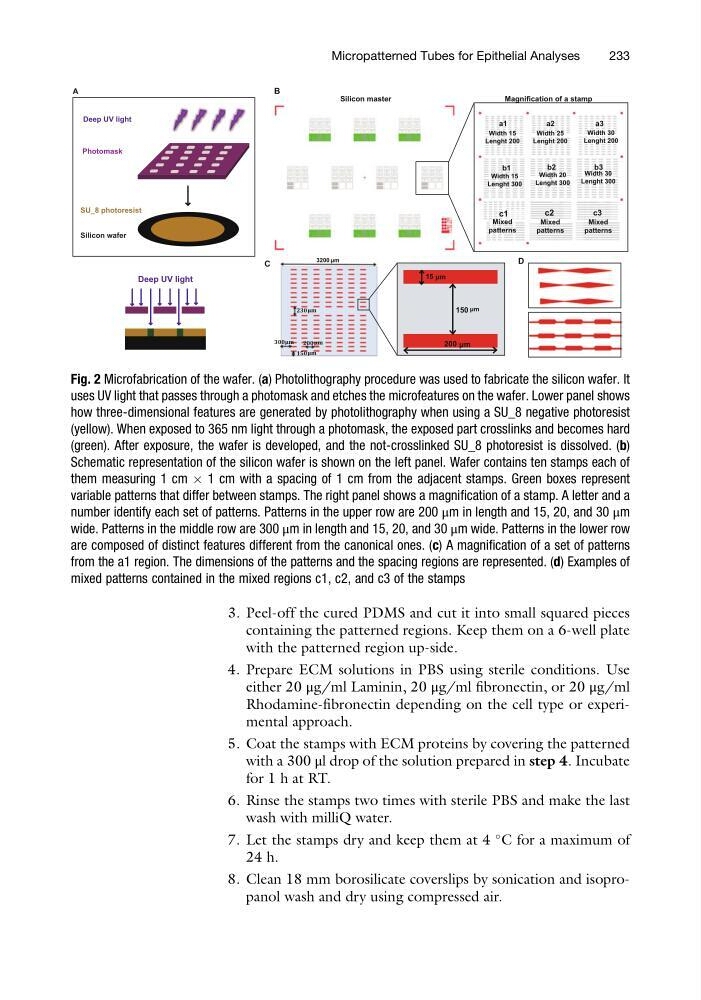
Fig. 2 Microfabrication of the wafer. (a) Photolithography procedure was used to fabricate the silicon wafer. It
uses UV light that passes through a photomask and etches the microfeatures on the wafer. Lower panel shows
how three-dimensional features are generated by photolithography when using a SU_8 negative photoresist
(yellow). When exposed to 365 nm light through a photomask, the exposed part crosslinks and becomes hard
(green). After exposure, the wafer is developed, and the not-crosslinked SU_8 photoresist is dissolved. (b)
Schematic representation of the silicon wafer is shown on the left panel. Wafer contains ten stamps each of
them measuring 1 cm  1 cm with a spacing of 1 cm from the adjacent stamps. Green boxes represent
variable patterns that differ between stamps. The right panel shows a magnification of a stamp. A letter and a
number identify each set of patterns. Patterns in the upper row are 200 μm in length and 15, 20, and 30 μm
wide. Patterns in the middle row are 300 μm in length and 15, 20, and 30 μm wide. Patterns in the lower row
are composed of distinct features different from the canonical ones. (c) A magnification of a set of patterns
from the a1 region. The dimensions of the patterns and the spacing regions are represented. (d) Examples of
mixed patterns contained in the mixed regions c1, c2, and c3 of the stamps
Micropatterned Tubes for Epithelial Analyses
233
containing the patterned regions. Keep them on a 6-well plate
with the patterned region up-side.
4. Prepare ECM solutions in PBS using sterile conditions. Use
either 20 μg/ml Laminin, 20 μg/ml fibronectin, or 20 μg/ml
Rhodamine-fibronectin depending on the cell type or experimental approach.
5. Coat the stamps with ECM proteins by covering the patterned
with a 300 μl drop of the solution prepared in step 4. Incubate
for 1 h at RT.
6. Rinse the stamps two times with sterile PBS and make the last
wash with milliQ water.
7. Let the stamps dry and keep them at 4
C for a maximum of
24 h.
8. Clean 18 mm borosilicate coverslips by sonication and isopropanol wash and dry using compressed air.
Deep UV light
Photomask
SU_8 photoresist
Silicon wafer
A
Deep UV light
B
Silicon master
Magnification of a stamp
a1
a2
b1
b3
b2
c1
c2
c3
230
200
300
150
3200
a3
Width 15
Lenght 200
Width 25
Lenght 200
Width 30
Lenght 200
Width 30
Lenght 300
Width 20
Lenght 300
Width 15
Lenght 300
Mixed
patterns
Mixed
patterns
Mixed
patterns
150
15
200
μm
μm
μm
μm
μm
μm
μm
μm
C
D
Fig. 2 Microfabrication of the wafer. (a) Photolithography procedure was used to fabricate the silicon wafer. It
uses UV light that passes through a photomask and etches the microfeatures on the wafer. Lower panel shows
how three-dimensional features are generated by photolithography when using a SU_8 negative photoresist
(yellow). When exposed to 365 nm light through a photomask, the exposed part crosslinks and becomes hard
(green). After exposure, the wafer is developed, and the not-crosslinked SU_8 photoresist is dissolved. (b)
Schematic representation of the silicon wafer is shown on the left panel. Wafer contains ten stamps each of
them measuring 1 cm  1 cm with a spacing of 1 cm from the adjacent stamps. Green boxes represent
variable patterns that differ between stamps. The right panel shows a magnification of a stamp. A letter and a
number identify each set of patterns. Patterns in the upper row are 200 μm in length and 15, 20, and 30 μm
wide. Patterns in the middle row are 300 μm in length and 15, 20, and 30 μm wide. Patterns in the lower row
are composed of distinct features different from the canonical ones. (c) A magnification of a set of patterns
from the a1 region. The dimensions of the patterns and the spacing regions are represented. (d) Examples of
mixed patterns contained in the mixed regions c1, c2, and c3 of the stamps
Micropatterned Tubes for Epithelial Analyses
233