

ECM-coated stamp. To perform μCP, a quartz photomask similar
to that used for photopatterning should be designed. For the
fabrication of photomasks and silicon wafers, please refer to [15]
(Fig. 2a). When designing the photomask, similar principles to
those used for the design of the photopatterning photomask
should be considered (Fig. 2b–d).
1. Use PDMS Sylgard184 to produce the stamps. Thoroughly
mix the elastomer and cross-linker components in a 1:10
(cross-linker: elastomer) ratio and keep under vacuum using a
vacuum bell or desiccator for 20–30 min to degas the mixture.
The amount of PDMS should be determined depending on the
number of stamps to fabricate.
2. Pour the PDMS over the silicon wafer and bake at 80
C for
1–2 h in the oven (see Notes 1 and 2).
A
B
Width
Length
Circular
Cap-less lines
S-shape
Capped lines
15
20
30
100
200
300
C
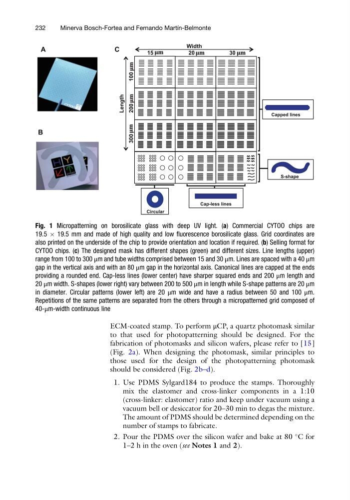
Fig. 1 Micropatterning on borosilicate glass with deep UV light. (a) Commercial CYTOO chips are
19.5 Â 19.5 mm and made of high quality and low fluorescence borosilicate glass. Grid coordinates are
also printed on the underside of the chip to provide orientation and location if required. (b) Selling format for
CYTOO chips. (c) The designed mask has different shapes (green) and different sizes. Line lengths (upper)
range from 100 to 300 μm and tube widths comprised between 15 and 30 μm. Lines are spaced with a 40 μm
gap in the vertical axis and with an 80 μm gap in the horizontal axis. Canonical lines are capped at the ends
providing a rounded end. Cap-less lines (lower center) have sharper squared ends and 200 μm length and
20 μm width. S-shapes (lower right) vary between 200 to 500 μm in length while S-shape patterns are 20 μm
in diameter. Circular patterns (lower left) are 20 μm wide and have a radius between 50 and 100 μm.
Repetitions of the same patterns are separated from the others through a micropatterned grid composed of
40-μm-width continuous line
232
Minerva Bosch-Fortea and Fernando Martı ´n-Belmonte
to that used for photopatterning should be designed. For the
fabrication of photomasks and silicon wafers, please refer to [15]
(Fig. 2a). When designing the photomask, similar principles to
those used for the design of the photopatterning photomask
should be considered (Fig. 2b–d).
1. Use PDMS Sylgard184 to produce the stamps. Thoroughly
mix the elastomer and cross-linker components in a 1:10
(cross-linker: elastomer) ratio and keep under vacuum using a
vacuum bell or desiccator for 20–30 min to degas the mixture.
The amount of PDMS should be determined depending on the
number of stamps to fabricate.
2. Pour the PDMS over the silicon wafer and bake at 80
C for
1–2 h in the oven (see Notes 1 and 2).
A
B
Width
Length
Circular
Cap-less lines
S-shape
Capped lines
15
20
30
100
200
300
C
Fig. 1 Micropatterning on borosilicate glass with deep UV light. (a) Commercial CYTOO chips are
19.5 Â 19.5 mm and made of high quality and low fluorescence borosilicate glass. Grid coordinates are
also printed on the underside of the chip to provide orientation and location if required. (b) Selling format for
CYTOO chips. (c) The designed mask has different shapes (green) and different sizes. Line lengths (upper)
range from 100 to 300 μm and tube widths comprised between 15 and 30 μm. Lines are spaced with a 40 μm
gap in the vertical axis and with an 80 μm gap in the horizontal axis. Canonical lines are capped at the ends
providing a rounded end. Cap-less lines (lower center) have sharper squared ends and 200 μm length and
20 μm width. S-shapes (lower right) vary between 200 to 500 μm in length while S-shape patterns are 20 μm
in diameter. Circular patterns (lower left) are 20 μm wide and have a radius between 50 and 100 μm.
Repetitions of the same patterns are separated from the others through a micropatterned grid composed of
40-μm-width continuous line
232
Minerva Bosch-Fortea and Fernando Martı ´n-Belmonte