

328
I. I. Smolyaninov and V. N. Smolyaninova
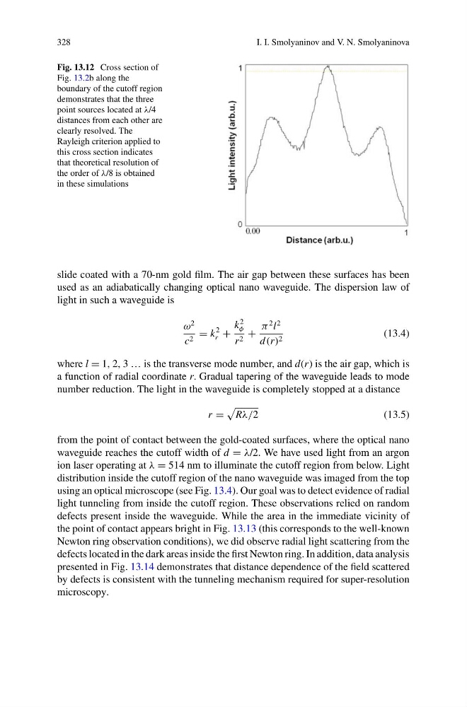
Fig. 13.12 Cross section of
Fig. 13.2b along the
boundary of the cutoff region
demonstrates that the three
point sources located at λ/4
distances from each other are
clearly resolved. The
Rayleigh criterion applied to
this cross section indicates
that theoretical resolution of
the order of λ/8 is obtained
in these simulations
slide coated with a 70-nm gold film. The air gap between these surfaces has been
used as an adiabatically changing optical nano waveguide. The dispersion law of
light in such a waveguide is
ω
2
c 2 = k
2
r +
k
2
φ
r 2 +
π
2 l
2
d (r) 2
(13.4)
where l = 1, 2, 3 … is the transverse mode number, and d(r) is the air gap, which is
a function of radial coordinate r. Gradual tapering of the waveguide leads to mode
number reduction. The light in the waveguide is completely stopped at a distance
r =
Rλ/2
(13.5)
from the point of contact between the gold-coated surfaces, where the optical nano
waveguide reaches the cutoff width of d = λ/2. We have used light from an argon
ion laser operating at λ = 514 nm to illuminate the cutoff region from below. Light
distribution inside the cutoff region of the nano waveguide was imaged from the top
using an optical microscope (see Fig. 13.4). Our goal was to detect evidence of radial
light tunneling from inside the cutoff region. These observations relied on random
defects present inside the waveguide. While the area in the immediate vicinity of
the point of contact appears bright in Fig. 13.13 (this corresponds to the well-known
Newton ring observation conditions), we did observe radial light scattering from the
defects located in the dark areas inside the first Newton ring. In addition, data analysis
presented in Fig. 13.14 demonstrates that distance dependence of the field scattered
by defects is consistent with the tunneling mechanism required for super-resolution
microscopy.
I. I. Smolyaninov and V. N. Smolyaninova
Fig. 13.12 Cross section of
Fig. 13.2b along the
boundary of the cutoff region
demonstrates that the three
point sources located at λ/4
distances from each other are
clearly resolved. The
Rayleigh criterion applied to
this cross section indicates
that theoretical resolution of
the order of λ/8 is obtained
in these simulations
slide coated with a 70-nm gold film. The air gap between these surfaces has been
used as an adiabatically changing optical nano waveguide. The dispersion law of
light in such a waveguide is
ω
2
c 2 = k
2
r +
k
2
φ
r 2 +
π
2 l
2
d (r) 2
(13.4)
where l = 1, 2, 3 … is the transverse mode number, and d(r) is the air gap, which is
a function of radial coordinate r. Gradual tapering of the waveguide leads to mode
number reduction. The light in the waveguide is completely stopped at a distance
r =
Rλ/2
(13.5)
from the point of contact between the gold-coated surfaces, where the optical nano
waveguide reaches the cutoff width of d = λ/2. We have used light from an argon
ion laser operating at λ = 514 nm to illuminate the cutoff region from below. Light
distribution inside the cutoff region of the nano waveguide was imaged from the top
using an optical microscope (see Fig. 13.4). Our goal was to detect evidence of radial
light tunneling from inside the cutoff region. These observations relied on random
defects present inside the waveguide. While the area in the immediate vicinity of
the point of contact appears bright in Fig. 13.13 (this corresponds to the well-known
Newton ring observation conditions), we did observe radial light scattering from the
defects located in the dark areas inside the first Newton ring. In addition, data analysis
presented in Fig. 13.14 demonstrates that distance dependence of the field scattered
by defects is consistent with the tunneling mechanism required for super-resolution
microscopy.