

9 Usage of Silicon for Label-Free Super-Resolved Imaging
229
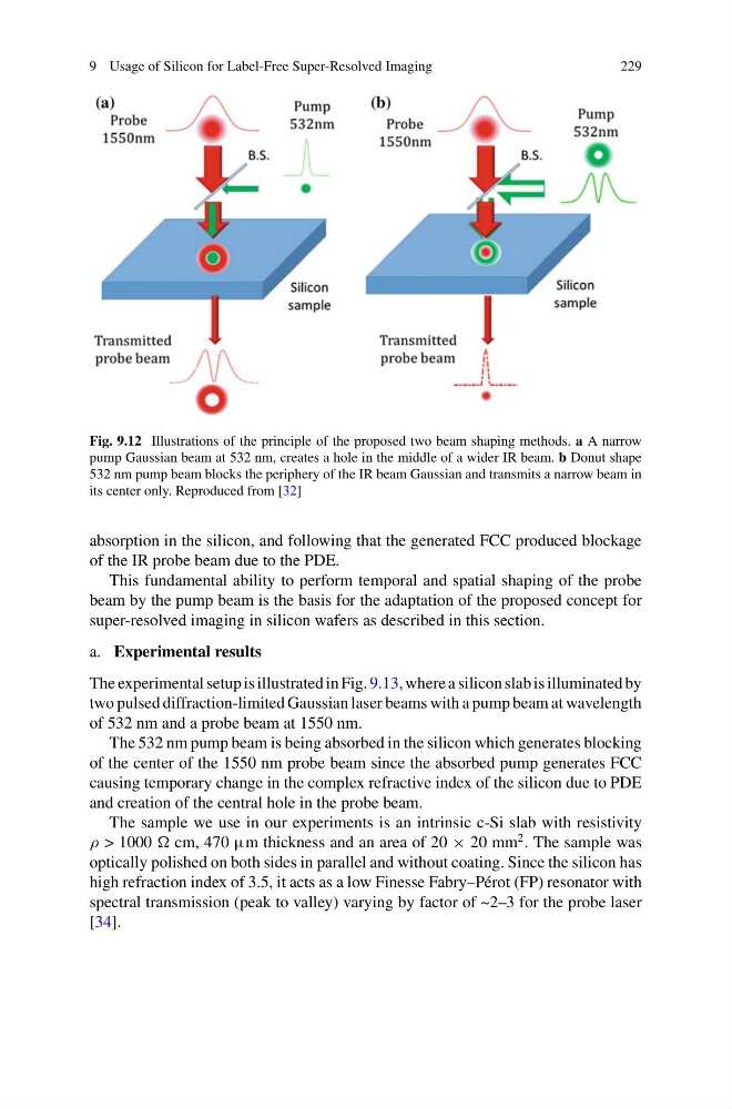
Fig. 9.12 Illustrations of the principle of the proposed two beam shaping methods. a A narrow
pump Gaussian beam at 532 nm, creates a hole in the middle of a wider IR beam. b Donut shape
532 nm pump beam blocks the periphery of the IR beam Gaussian and transmits a narrow beam in
its center only. Reproduced from [32]
absorption in the silicon, and following that the generated FCC produced blockage
of the IR probe beam due to the PDE.
This fundamental ability to perform temporal and spatial shaping of the probe
beam by the pump beam is the basis for the adaptation of the proposed concept for
super-resolved imaging in silicon wafers as described in this section.
a. Experimental results
The experimental setup is illustrated in Fig. 9.13, where a silicon slab is illuminated by
two pulsed diffraction-limited Gaussian laser beams with a pump beam at wavelength
of 532 nm and a probe beam at 1550 nm.
The 532 nm pump beam is being absorbed in the silicon which generates blocking
of the center of the 1550 nm probe beam since the absorbed pump generates FCC
causing temporary change in the complex refractive index of the silicon due to PDE
and creation of the central hole in the probe beam.
The sample we use in our experiments is an intrinsic c-Si slab with resistivity
ρ > 1000 cm, 470 μm thickness and an area of 20 × 20 mm
2 . The sample was
optically polished on both sides in parallel and without coating. Since the silicon has
high refraction index of 3.5, it acts as a low Finesse Fabry–Pérot (FP) resonator with
spectral transmission (peak to valley) varying by factor of ~2–3 for the probe laser
[34].
229
Fig. 9.12 Illustrations of the principle of the proposed two beam shaping methods. a A narrow
pump Gaussian beam at 532 nm, creates a hole in the middle of a wider IR beam. b Donut shape
532 nm pump beam blocks the periphery of the IR beam Gaussian and transmits a narrow beam in
its center only. Reproduced from [32]
absorption in the silicon, and following that the generated FCC produced blockage
of the IR probe beam due to the PDE.
This fundamental ability to perform temporal and spatial shaping of the probe
beam by the pump beam is the basis for the adaptation of the proposed concept for
super-resolved imaging in silicon wafers as described in this section.
a. Experimental results
The experimental setup is illustrated in Fig. 9.13, where a silicon slab is illuminated by
two pulsed diffraction-limited Gaussian laser beams with a pump beam at wavelength
of 532 nm and a probe beam at 1550 nm.
The 532 nm pump beam is being absorbed in the silicon which generates blocking
of the center of the 1550 nm probe beam since the absorbed pump generates FCC
causing temporary change in the complex refractive index of the silicon due to PDE
and creation of the central hole in the probe beam.
The sample we use in our experiments is an intrinsic c-Si slab with resistivity
ρ > 1000 cm, 470 μm thickness and an area of 20 × 20 mm
2 . The sample was
optically polished on both sides in parallel and without coating. Since the silicon has
high refraction index of 3.5, it acts as a low Finesse Fabry–Pérot (FP) resonator with
spectral transmission (peak to valley) varying by factor of ~2–3 for the probe laser
[34].