

9 Usage of Silicon for Label-Free Super-Resolved Imaging
227
CRESTEC CABLE-9000C, a high-resolution electron-beam lithography system,
was used to expose the PMMA layer to different irradiation doses and right after the
sample was developed for 50 seconds by MIBK (methyl-isobutyl-ketone) and rinsed
with IPA.
Following this, the sample was dispositioned with 10 nm Au and 3 nm chrome. For
the resist liftoff, the sample was immersed in acetone at 100 kHz ultrasonic bath for
3 h. The fabrication process ended up with deposition of more 10 nm silicon using
BESTEC 2
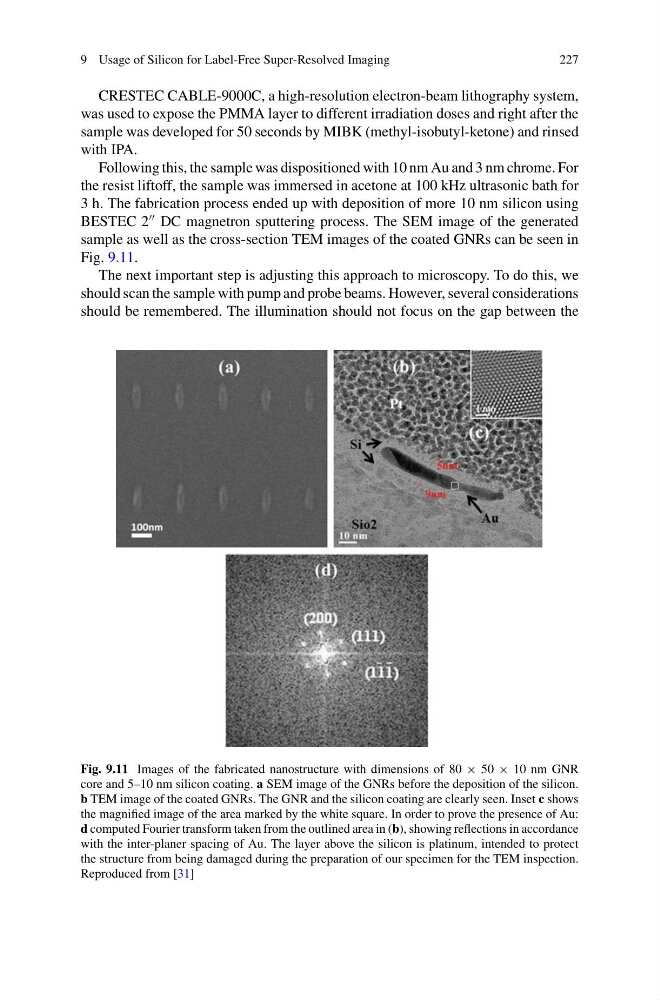
DC magnetron sputtering process. The SEM image of the generated
sample as well as the cross-section TEM images of the coated GNRs can be seen in
Fig. 9.11.
The next important step is adjusting this approach to microscopy. To do this, we
should scan the sample with pump and probe beams. However, several considerations
should be remembered. The illumination should not focus on the gap between the
Fig. 9.11 Images of the fabricated nanostructure with dimensions of 80 × 50 × 10 nm GNR
core and 5–10 nm silicon coating. a SEM image of the GNRs before the deposition of the silicon.
b TEM image of the coated GNRs. The GNR and the silicon coating are clearly seen. Inset c shows
the magnified image of the area marked by the white square. In order to prove the presence of Au:
d computed Fourier transform taken from the outlined area in (b), showing reflections in accordance
with the inter-planer spacing of Au. The layer above the silicon is platinum, intended to protect
the structure from being damaged during the preparation of our specimen for the TEM inspection.
Reproduced from [31]
227
CRESTEC CABLE-9000C, a high-resolution electron-beam lithography system,
was used to expose the PMMA layer to different irradiation doses and right after the
sample was developed for 50 seconds by MIBK (methyl-isobutyl-ketone) and rinsed
with IPA.
Following this, the sample was dispositioned with 10 nm Au and 3 nm chrome. For
the resist liftoff, the sample was immersed in acetone at 100 kHz ultrasonic bath for
3 h. The fabrication process ended up with deposition of more 10 nm silicon using
BESTEC 2
DC magnetron sputtering process. The SEM image of the generated
sample as well as the cross-section TEM images of the coated GNRs can be seen in
Fig. 9.11.
The next important step is adjusting this approach to microscopy. To do this, we
should scan the sample with pump and probe beams. However, several considerations
should be remembered. The illumination should not focus on the gap between the
Fig. 9.11 Images of the fabricated nanostructure with dimensions of 80 × 50 × 10 nm GNR
core and 5–10 nm silicon coating. a SEM image of the GNRs before the deposition of the silicon.
b TEM image of the coated GNRs. The GNR and the silicon coating are clearly seen. Inset c shows
the magnified image of the area marked by the white square. In order to prove the presence of Au:
d computed Fourier transform taken from the outlined area in (b), showing reflections in accordance
with the inter-planer spacing of Au. The layer above the silicon is platinum, intended to protect
the structure from being damaged during the preparation of our specimen for the TEM inspection.
Reproduced from [31]