

222
H. Pinhas et al.
9.4 Enhancement of the Effect
In this section we show how the effect described in the previous section can be
enhanced by properly designing the shape of the silicon-based nanostructures [31].
The idea is to use metallic structures that are encapsulating the silicon, having edges
that can enhance the electrical field density.
a. Method
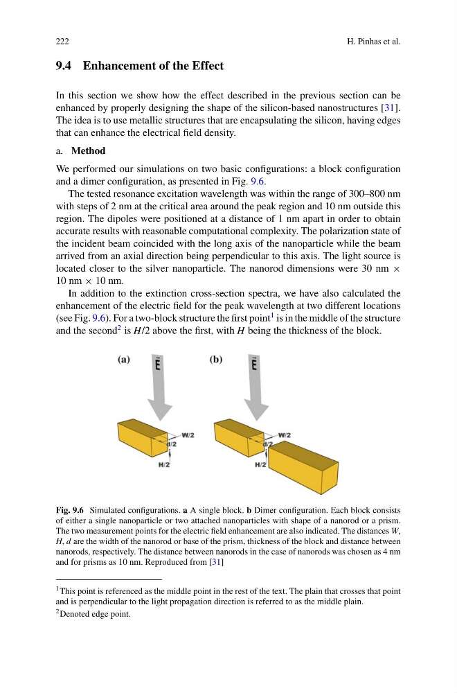
We performed our simulations on two basic configurations: a block configuration
and a dimer configuration, as presented in Fig. 9.6.
The tested resonance excitation wavelength was within the range of 300–800 nm
with steps of 2 nm at the critical area around the peak region and 10 nm outside this
region. The dipoles were positioned at a distance of 1 nm apart in order to obtain
accurate results with reasonable computational complexity. The polarization state of
the incident beam coincided with the long axis of the nanoparticle while the beam
arrived from an axial direction being perpendicular to this axis. The light source is
located closer to the silver nanoparticle. The nanorod dimensions were 30 nm ×
10 nm × 10 nm.
In addition to the extinction cross-section spectra, we have also calculated the
enhancement of the electric field for the peak wavelength at two different locations
(see Fig. 9.6). For a two-block structure the first point
1 is in the middle of the structure
and the second
2 is H/2 above the first, with H being the thickness of the block.
Fig. 9.6 Simulated configurations. a A single block. b Dimer configuration. Each block consists
of either a single nanoparticle or two attached nanoparticles with shape of a nanorod or a prism.
The two measurement points for the electric field enhancement are also indicated. The distances W,
H, d are the width of the nanorod or base of the prism, thickness of the block and distance between
nanorods, respectively. The distance between nanorods in the case of nanorods was chosen as 4 nm
and for prisms as 10 nm. Reproduced from [31]
1 This point is referenced as the middle point in the rest of the text. The plain that crosses that point
and is perpendicular to the light propagation direction is referred to as the middle plain.
2 Denoted edge point.
H. Pinhas et al.
9.4 Enhancement of the Effect
In this section we show how the effect described in the previous section can be
enhanced by properly designing the shape of the silicon-based nanostructures [31].
The idea is to use metallic structures that are encapsulating the silicon, having edges
that can enhance the electrical field density.
a. Method
We performed our simulations on two basic configurations: a block configuration
and a dimer configuration, as presented in Fig. 9.6.
The tested resonance excitation wavelength was within the range of 300–800 nm
with steps of 2 nm at the critical area around the peak region and 10 nm outside this
region. The dipoles were positioned at a distance of 1 nm apart in order to obtain
accurate results with reasonable computational complexity. The polarization state of
the incident beam coincided with the long axis of the nanoparticle while the beam
arrived from an axial direction being perpendicular to this axis. The light source is
located closer to the silver nanoparticle. The nanorod dimensions were 30 nm ×
10 nm × 10 nm.
In addition to the extinction cross-section spectra, we have also calculated the
enhancement of the electric field for the peak wavelength at two different locations
(see Fig. 9.6). For a two-block structure the first point
1 is in the middle of the structure
and the second
2 is H/2 above the first, with H being the thickness of the block.
Fig. 9.6 Simulated configurations. a A single block. b Dimer configuration. Each block consists
of either a single nanoparticle or two attached nanoparticles with shape of a nanorod or a prism.
The two measurement points for the electric field enhancement are also indicated. The distances W,
H, d are the width of the nanorod or base of the prism, thickness of the block and distance between
nanorods, respectively. The distance between nanorods in the case of nanorods was chosen as 4 nm
and for prisms as 10 nm. Reproduced from [31]
1 This point is referenced as the middle point in the rest of the text. The plain that crosses that point
and is perpendicular to the light propagation direction is referred to as the middle plain.
2 Denoted edge point.