

9 Usage of Silicon for Label-Free Super-Resolved Imaging
215
electronics industry. Note that the silicon nanostructures have a growing interest
[21–23] and are fabrication-feasible.
Our final aim is to create a non-fluorescent label-free nanoscope that will be
extremely applicable to the field of imaging, either biomedical or in failure analysis.
In the case of biomedical imaging, the concept involves the illumination of objects
tagged with high concentrated silicon-coated GNRs. The method uses two lasers for
illumination; a high-intensity pump beam and a probe beam that is spatially aligned
with the pump beam. The high-intensity pump beam generates electrons and holes
pairs in the silicon shell and thus yields a change in the refractive index of the silicon
shell, via the PDE. Owing to the PDE, the real part of the refractive index reduces,
while the imaginary part grows. As a result, the silicon shell becomes more metallic.
Since the laser illumination profile has a Gaussian shape, the refractive index change
will be more dominant near the Gaussian peak. As a result, the LSPR of the coated
GNRs will shift due to modification of the effective radius and aspect ratio of the
structure. The probe beam (which is in the near infra-red wavelength) is fixed to the
plasmonic resonance of this nanostructure without applying the pump illumination.
The pump beam shifts the LSPR in accordance to the spatial location inside the
Gaussian beam. The refractive index change caused by the pump is transformed
into a change in the profile of the PSF and this modified PSF has a doughnut-like
shape that contains higher spatial frequencies (i.e. sub-wavelength spatial features)
compared to a regular Gaussian PSF. Scanning a sample with this elaborated PSF
can reconstruct higher spatial frequencies within the inspected sample and obtain a
sub-wavelength super-resolution image.
In the case of silicon wafers for failure analysis application, the optical configuration is the same but no metallic coating is used. In the case of wafers, one of the
main advantages is the capability to perform a super-resolved imaging deep into the
wafer and not only on its surface by using temporally pulsed pump illumination.
9.2 Theoretical Background
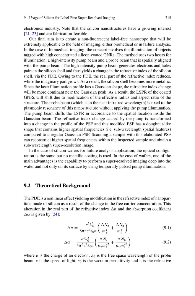
The PDE is a nonlinear effect yielding modification in the refractive index of nanoparticle made of silicon as a result of the change in the free carrier concentration. This
alteration in the real part of the refractive index n and the absorption coefficient
α is given by [24]:
n =
−e
2
λ
2
0
8π 2 c 2 ε 0 n
N e
m ∗
e
+
N h
m
∗
h
(9.1)
α =
e
3
λ
2
0
4π 2 c 3 ε 0 n
N e
μ e m ∗2
e
+
N h
μ h m
∗2
h
(9.2)
where e is the charge of an electron, λ 0 is the free space wavelength of the probe
beam, c is the speed of light, ε 0 is the vacuum permittivity and n is the refractive
215
electronics industry. Note that the silicon nanostructures have a growing interest
[21–23] and are fabrication-feasible.
Our final aim is to create a non-fluorescent label-free nanoscope that will be
extremely applicable to the field of imaging, either biomedical or in failure analysis.
In the case of biomedical imaging, the concept involves the illumination of objects
tagged with high concentrated silicon-coated GNRs. The method uses two lasers for
illumination; a high-intensity pump beam and a probe beam that is spatially aligned
with the pump beam. The high-intensity pump beam generates electrons and holes
pairs in the silicon shell and thus yields a change in the refractive index of the silicon
shell, via the PDE. Owing to the PDE, the real part of the refractive index reduces,
while the imaginary part grows. As a result, the silicon shell becomes more metallic.
Since the laser illumination profile has a Gaussian shape, the refractive index change
will be more dominant near the Gaussian peak. As a result, the LSPR of the coated
GNRs will shift due to modification of the effective radius and aspect ratio of the
structure. The probe beam (which is in the near infra-red wavelength) is fixed to the
plasmonic resonance of this nanostructure without applying the pump illumination.
The pump beam shifts the LSPR in accordance to the spatial location inside the
Gaussian beam. The refractive index change caused by the pump is transformed
into a change in the profile of the PSF and this modified PSF has a doughnut-like
shape that contains higher spatial frequencies (i.e. sub-wavelength spatial features)
compared to a regular Gaussian PSF. Scanning a sample with this elaborated PSF
can reconstruct higher spatial frequencies within the inspected sample and obtain a
sub-wavelength super-resolution image.
In the case of silicon wafers for failure analysis application, the optical configuration is the same but no metallic coating is used. In the case of wafers, one of the
main advantages is the capability to perform a super-resolved imaging deep into the
wafer and not only on its surface by using temporally pulsed pump illumination.
9.2 Theoretical Background
The PDE is a nonlinear effect yielding modification in the refractive index of nanoparticle made of silicon as a result of the change in the free carrier concentration. This
alteration in the real part of the refractive index n and the absorption coefficient
α is given by [24]:
n =
−e
2
λ
2
0
8π 2 c 2 ε 0 n
N e
m ∗
e
+
N h
m
∗
h
(9.1)
α =
e
3
λ
2
0
4π 2 c 3 ε 0 n
N e
μ e m ∗2
e
+
N h
μ h m
∗2
h
(9.2)
where e is the charge of an electron, λ 0 is the free space wavelength of the probe
beam, c is the speed of light, ε 0 is the vacuum permittivity and n is the refractive