

at which point milling should be stopped (e.g., lamella bending/
bulging, loss of GIS platinum layer, or holes in the lamella from
uneven milling).
1. Bring a selected milling target to the beam-coincidence point
(see Note 12). Make sure sample is at desired tilt (see Subheadings 1.2 and 3.1) to determine appropriate milling angle).
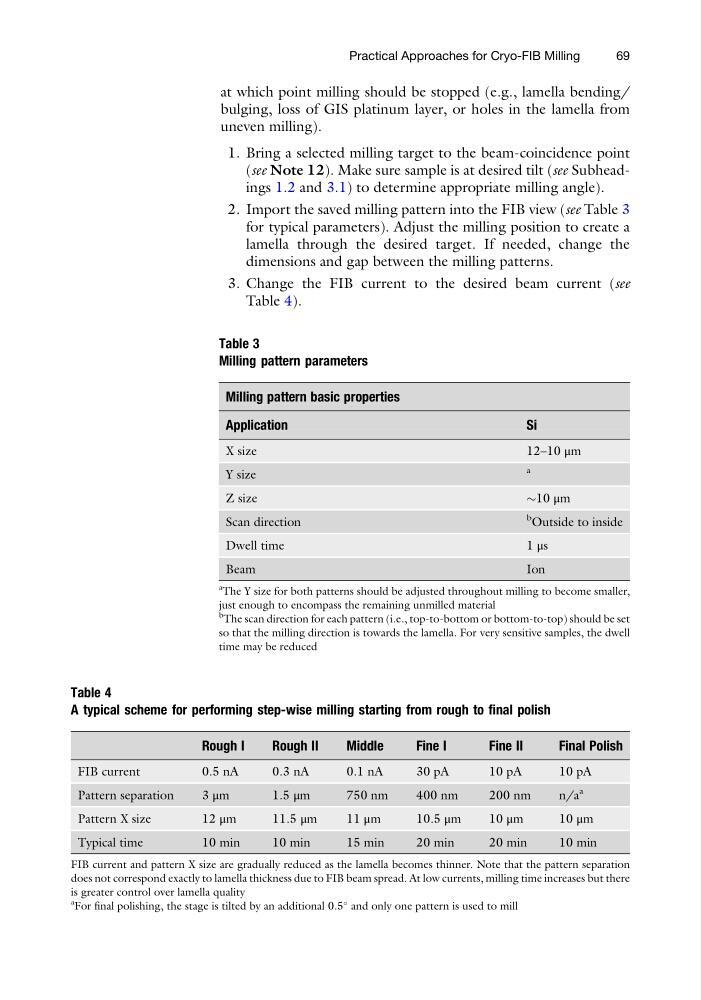
2. Import the saved milling pattern into the FIB view (see Table 3
for typical parameters). Adjust the milling position to create a
lamella through the desired target. If needed, change the
dimensions and gap between the milling patterns.
3. Change the FIB current to the desired beam current (see
Table 4).
Table 3
Milling pattern parameters
Milling pattern basic properties
Application
Si
X size
12–10 μm
Y size
a
Z size
$10 μm
Scan direction
b Outside to inside
Dwell time
1 μs
Beam
Ion
a
The Y size for both patterns should be adjusted throughout milling to become smaller,
just enough to encompass the remaining unmilled material
b
The scan direction for each pattern (i.e., top-to-bottom or bottom-to-top) should be set
so that the milling direction is towards the lamella. For very sensitive samples, the dwell
time may be reduced
Table 4
A typical scheme for performing step-wise milling starting from rough to final polish
Rough I
Rough II
Middle
Fine I
Fine II
Final Polish
FIB current
0.5 nA
0.3 nA
0.1 nA
30 pA
10 pA
10 pA
Pattern separation
3 μm
1.5 μm
750 nm
400 nm
200 nm
n/a
a
Pattern X size
12 μm
11.5 μm
11μm
10.5 μm
10μm
1 0μm
Typical time
10 min
10 min
15 min
20 min
20 min
10 min
FIB current and pattern X size are gradually reduced as the lamella becomes thinner. Note that the pattern separation
does not correspond exactly to lamella thickness due to FIB beam spread. At low currents, milling time increases but there
is greater control over lamella quality
a
For final polishing, the stage is tilted by an additional 0.5
and only one pattern is used to mill
Practical Approaches for Cryo-FIB Milling
69
bulging, loss of GIS platinum layer, or holes in the lamella from
uneven milling).
1. Bring a selected milling target to the beam-coincidence point
(see Note 12). Make sure sample is at desired tilt (see Subheadings 1.2 and 3.1) to determine appropriate milling angle).
2. Import the saved milling pattern into the FIB view (see Table 3
for typical parameters). Adjust the milling position to create a
lamella through the desired target. If needed, change the
dimensions and gap between the milling patterns.
3. Change the FIB current to the desired beam current (see
Table 4).
Table 3
Milling pattern parameters
Milling pattern basic properties
Application
Si
X size
12–10 μm
Y size
a
Z size
$10 μm
Scan direction
b Outside to inside
Dwell time
1 μs
Beam
Ion
a
The Y size for both patterns should be adjusted throughout milling to become smaller,
just enough to encompass the remaining unmilled material
b
The scan direction for each pattern (i.e., top-to-bottom or bottom-to-top) should be set
so that the milling direction is towards the lamella. For very sensitive samples, the dwell
time may be reduced
Table 4
A typical scheme for performing step-wise milling starting from rough to final polish
Rough I
Rough II
Middle
Fine I
Fine II
Final Polish
FIB current
0.5 nA
0.3 nA
0.1 nA
30 pA
10 pA
10 pA
Pattern separation
3 μm
1.5 μm
750 nm
400 nm
200 nm
n/a
a
Pattern X size
12 μm
11.5 μm
11μm
10.5 μm
10μm
1 0μm
Typical time
10 min
10 min
15 min
20 min
20 min
10 min
FIB current and pattern X size are gradually reduced as the lamella becomes thinner. Note that the pattern separation
does not correspond exactly to lamella thickness due to FIB beam spread. At low currents, milling time increases but there
is greater control over lamella quality
a
For final polishing, the stage is tilted by an additional 0.5
and only one pattern is used to mill
Practical Approaches for Cryo-FIB Milling
69