

30
M. I. Stockman
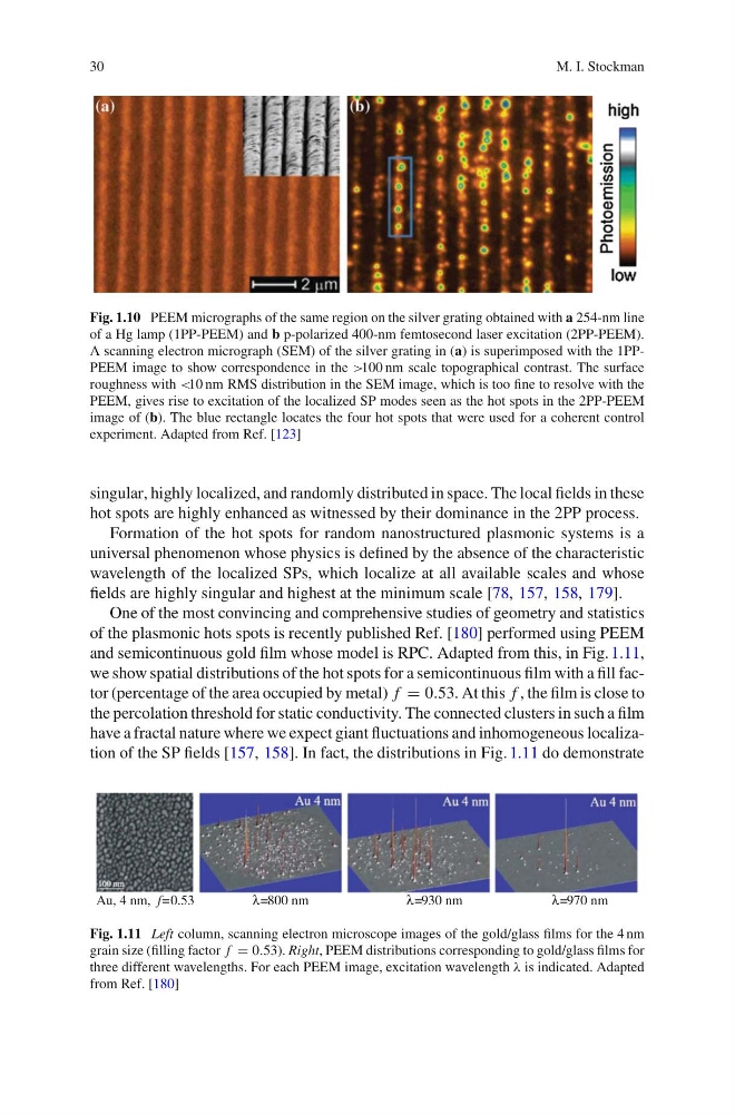
Fig. 1.10 PEEM micrographs of the same region on the silver grating obtained with a 254-nm line
of a Hg lamp (1PP-PEEM) and b p-polarized 400-nm femtosecond laser excitation (2PP-PEEM).
A scanning electron micrograph (SEM) of the silver grating in (a) is superimposed with the 1PPPEEM image to show correspondence in the >100 nm scale topographical contrast. The surface
roughness with <10 nm RMS distribution in the SEM image, which is too fine to resolve with the
PEEM, gives rise to excitation of the localized SP modes seen as the hot spots in the 2PP-PEEM
image of (b). The blue rectangle locates the four hot spots that were used for a coherent control
experiment. Adapted from Ref. [123]
singular, highly localized, and randomly distributed in space. The local fields in these
hot spots are highly enhanced as witnessed by their dominance in the 2PP process.
Formation of the hot spots for random nanostructured plasmonic systems is a
universal phenomenon whose physics is defined by the absence of the characteristic
wavelength of the localized SPs, which localize at all available scales and whose
fields are highly singular and highest at the minimum scale [78, 157, 158, 179].
One of the most convincing and comprehensive studies of geometry and statistics
of the plasmonic hots spots is recently published Ref. [180] performed using PEEM
and semicontinuous gold film whose model is RPC. Adapted from this, in Fig. 1.11,
we show spatial distributions of the hot spots for a semicontinuous film with a fill factor (percentage of the area occupied by metal) f = 0.53. At this f , the film is close to
the percolation threshold for static conductivity. The connected clusters in such a film
have a fractal nature where we expect giant fluctuations and inhomogeneous localization of the SP fields [157, 158]. In fact, the distributions in Fig. 1.11 do demonstrate
Au, 4 nm, f=0.53
λ=800 nm
λ=930 nm
λ=970 nm
Fig. 1.11 Left column, scanning electron microscope images of the gold/glass films for the 4 nm
grain size (filling factor f = 0.53). Right, PEEM distributions corresponding to gold/glass films for
three different wavelengths. For each PEEM image, excitation wavelength λ is indicated. Adapted
from Ref. [180]
M. I. Stockman
Fig. 1.10 PEEM micrographs of the same region on the silver grating obtained with a 254-nm line
of a Hg lamp (1PP-PEEM) and b p-polarized 400-nm femtosecond laser excitation (2PP-PEEM).
A scanning electron micrograph (SEM) of the silver grating in (a) is superimposed with the 1PPPEEM image to show correspondence in the >100 nm scale topographical contrast. The surface
roughness with <10 nm RMS distribution in the SEM image, which is too fine to resolve with the
PEEM, gives rise to excitation of the localized SP modes seen as the hot spots in the 2PP-PEEM
image of (b). The blue rectangle locates the four hot spots that were used for a coherent control
experiment. Adapted from Ref. [123]
singular, highly localized, and randomly distributed in space. The local fields in these
hot spots are highly enhanced as witnessed by their dominance in the 2PP process.
Formation of the hot spots for random nanostructured plasmonic systems is a
universal phenomenon whose physics is defined by the absence of the characteristic
wavelength of the localized SPs, which localize at all available scales and whose
fields are highly singular and highest at the minimum scale [78, 157, 158, 179].
One of the most convincing and comprehensive studies of geometry and statistics
of the plasmonic hots spots is recently published Ref. [180] performed using PEEM
and semicontinuous gold film whose model is RPC. Adapted from this, in Fig. 1.11,
we show spatial distributions of the hot spots for a semicontinuous film with a fill factor (percentage of the area occupied by metal) f = 0.53. At this f , the film is close to
the percolation threshold for static conductivity. The connected clusters in such a film
have a fractal nature where we expect giant fluctuations and inhomogeneous localization of the SP fields [157, 158]. In fact, the distributions in Fig. 1.11 do demonstrate
Au, 4 nm, f=0.53
λ=800 nm
λ=930 nm
λ=970 nm
Fig. 1.11 Left column, scanning electron microscope images of the gold/glass films for the 4 nm
grain size (filling factor f = 0.53). Right, PEEM distributions corresponding to gold/glass films for
three different wavelengths. For each PEEM image, excitation wavelength λ is indicated. Adapted
from Ref. [180]