

9 Aperiodic Order in Nanoplasmonics
369
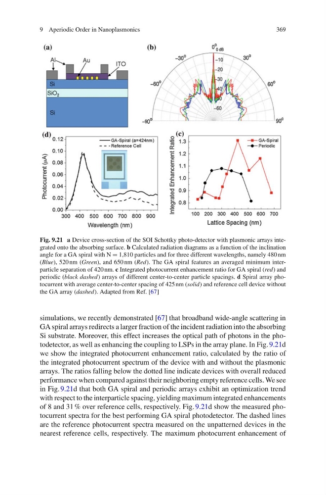
Fig. 9.21 a Device cross-section of the SOI Schottky photo-detector with plasmonic arrays integrated onto the absorbing surface. b Calculated radiation diagrams as a function of the inclination
angle for a GA spiral with N = 1,810 particles and for three different wavelengths, namely 480 nm
(Blue), 520 nm (Green), and 650 nm (Red). The GA spiral features an averaged minimum interparticle separation of 420 nm. c Integrated photocurrent enhancement ratio for GA spiral (red) and
periodic (black dashed) arrays of different center-to-center particle spacings. d Spiral array photocurrent with average center-to-center spacing of 425 nm (solid) and reference cell device without
the GA array (dashed). Adapted from Ref. [67]
simulations, we recently demonstrated [67] that broadband wide-angle scattering in
GA spiral arrays redirects a larger fraction of the incident radiation into the absorbing
Si substrate. Moreover, this effect increases the optical path of photons in the photodetector, as well as enhancing the coupling to LSPs in the array plane. In Fig. 9.21d
we show the integrated photocurrent enhancement ratio, calculated by the ratio of
the integrated photocurrent spectrum of the device with and without the plasmonic
arrays. The ratios falling below the dotted line indicate devices with overall reduced
performance when compared against their neighboring empty reference cells. We see
in Fig. 9.21d that both GA spiral and periodic arrays exhibit an optimization trend
with respect to the interparticle spacing, yielding maximum integrated enhancements
of 8 and 31 % over reference cells, respectively. Fig. 9.21d show the measured photocurrent spectra for the best performing GA spiral photodetector. The dashed lines
are the reference photocurrent spectra measured on the unpatterned devices in the
nearest reference cells, respectively. The maximum photocurrent enhancement of
369
Fig. 9.21 a Device cross-section of the SOI Schottky photo-detector with plasmonic arrays integrated onto the absorbing surface. b Calculated radiation diagrams as a function of the inclination
angle for a GA spiral with N = 1,810 particles and for three different wavelengths, namely 480 nm
(Blue), 520 nm (Green), and 650 nm (Red). The GA spiral features an averaged minimum interparticle separation of 420 nm. c Integrated photocurrent enhancement ratio for GA spiral (red) and
periodic (black dashed) arrays of different center-to-center particle spacings. d Spiral array photocurrent with average center-to-center spacing of 425 nm (solid) and reference cell device without
the GA array (dashed). Adapted from Ref. [67]
simulations, we recently demonstrated [67] that broadband wide-angle scattering in
GA spiral arrays redirects a larger fraction of the incident radiation into the absorbing
Si substrate. Moreover, this effect increases the optical path of photons in the photodetector, as well as enhancing the coupling to LSPs in the array plane. In Fig. 9.21d
we show the integrated photocurrent enhancement ratio, calculated by the ratio of
the integrated photocurrent spectrum of the device with and without the plasmonic
arrays. The ratios falling below the dotted line indicate devices with overall reduced
performance when compared against their neighboring empty reference cells. We see
in Fig. 9.21d that both GA spiral and periodic arrays exhibit an optimization trend
with respect to the interparticle spacing, yielding maximum integrated enhancements
of 8 and 31 % over reference cells, respectively. Fig. 9.21d show the measured photocurrent spectra for the best performing GA spiral photodetector. The dashed lines
are the reference photocurrent spectra measured on the unpatterned devices in the
nearest reference cells, respectively. The maximum photocurrent enhancement of