

9 Aperiodic Order in Nanoplasmonics
355
probe microscopy (SPM), suffer from high operating costs and low throughput. On
the other hand, shadow-mask patterning techniques, such as stencil-based methods,
allow for the fabrication of plasmonic nanostructures but inherently suffer from edge
blurring and cannot produce plasmonic films perforated with nano-holes, which play
an important role in nanoplasmonics.
To solve these problems, we recently proposed and demonstrated a scalable and
cost-effective direct transfer nanofabrication technique that utilizes a hard mold master and an inexpensive, commercially available flip-chip bonder, for the fabrication
of large-scale metallic nanoparticles and perforated metallic films (plasmonic nanohole arrays) directly atop silk fibroin films [98].
The process flow for the transfer imprint of plasmonic nano-dots and nano-holes,
begins with the fabrication of the reusable master molds. As an example, we discuss
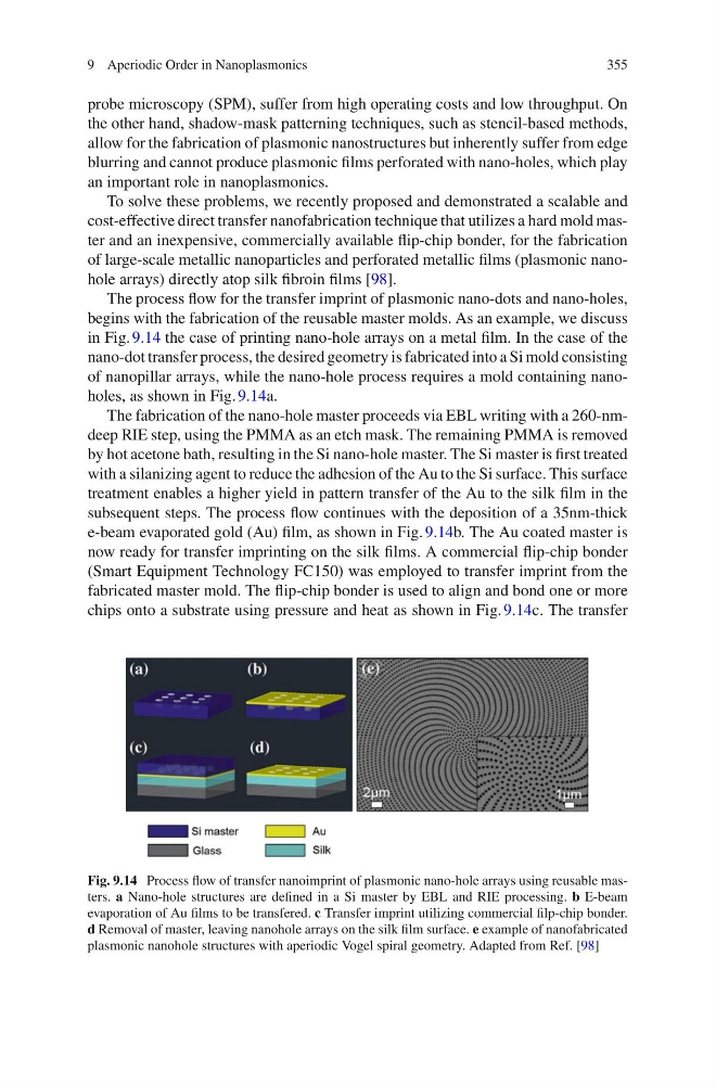
in Fig. 9.14 the case of printing nano-hole arrays on a metal film. In the case of the
nano-dot transfer process, the desired geometry is fabricated into a Si mold consisting
of nanopillar arrays, while the nano-hole process requires a mold containing nanoholes, as shown in Fig. 9.14a.
The fabrication of the nano-hole master proceeds via EBL writing with a 260-nmdeep RIE step, using the PMMA as an etch mask. The remaining PMMA is removed
by hot acetone bath, resulting in the Si nano-hole master. The Si master is first treated
with a silanizing agent to reduce the adhesion of the Au to the Si surface. This surface
treatment enables a higher yield in pattern transfer of the Au to the silk film in the
subsequent steps. The process flow continues with the deposition of a 35nm-thick
e-beam evaporated gold (Au) film, as shown in Fig. 9.14b. The Au coated master is
now ready for transfer imprinting on the silk films. A commercial flip-chip bonder
(Smart Equipment Technology FC150) was employed to transfer imprint from the
fabricated master mold. The flip-chip bonder is used to align and bond one or more
chips onto a substrate using pressure and heat as shown in Fig. 9.14c. The transfer
Fig. 9.14 Process flow of transfer nanoimprint of plasmonic nano-hole arrays using reusable masters. a Nano-hole structures are defined in a Si master by EBL and RIE processing. b E-beam
evaporation of Au films to be transfered. c Transfer imprint utilizing commercial filp-chip bonder.
d Removal of master, leaving nanohole arrays on the silk film surface. e example of nanofabricated
plasmonic nanohole structures with aperiodic Vogel spiral geometry. Adapted from Ref. [98]
355
probe microscopy (SPM), suffer from high operating costs and low throughput. On
the other hand, shadow-mask patterning techniques, such as stencil-based methods,
allow for the fabrication of plasmonic nanostructures but inherently suffer from edge
blurring and cannot produce plasmonic films perforated with nano-holes, which play
an important role in nanoplasmonics.
To solve these problems, we recently proposed and demonstrated a scalable and
cost-effective direct transfer nanofabrication technique that utilizes a hard mold master and an inexpensive, commercially available flip-chip bonder, for the fabrication
of large-scale metallic nanoparticles and perforated metallic films (plasmonic nanohole arrays) directly atop silk fibroin films [98].
The process flow for the transfer imprint of plasmonic nano-dots and nano-holes,
begins with the fabrication of the reusable master molds. As an example, we discuss
in Fig. 9.14 the case of printing nano-hole arrays on a metal film. In the case of the
nano-dot transfer process, the desired geometry is fabricated into a Si mold consisting
of nanopillar arrays, while the nano-hole process requires a mold containing nanoholes, as shown in Fig. 9.14a.
The fabrication of the nano-hole master proceeds via EBL writing with a 260-nmdeep RIE step, using the PMMA as an etch mask. The remaining PMMA is removed
by hot acetone bath, resulting in the Si nano-hole master. The Si master is first treated
with a silanizing agent to reduce the adhesion of the Au to the Si surface. This surface
treatment enables a higher yield in pattern transfer of the Au to the silk film in the
subsequent steps. The process flow continues with the deposition of a 35nm-thick
e-beam evaporated gold (Au) film, as shown in Fig. 9.14b. The Au coated master is
now ready for transfer imprinting on the silk films. A commercial flip-chip bonder
(Smart Equipment Technology FC150) was employed to transfer imprint from the
fabricated master mold. The flip-chip bonder is used to align and bond one or more
chips onto a substrate using pressure and heat as shown in Fig. 9.14c. The transfer
Fig. 9.14 Process flow of transfer nanoimprint of plasmonic nano-hole arrays using reusable masters. a Nano-hole structures are defined in a Si master by EBL and RIE processing. b E-beam
evaporation of Au films to be transfered. c Transfer imprint utilizing commercial filp-chip bonder.
d Removal of master, leaving nanohole arrays on the silk film surface. e example of nanofabricated
plasmonic nanohole structures with aperiodic Vogel spiral geometry. Adapted from Ref. [98]