

9 Aperiodic Order in Nanoplasmonics
353
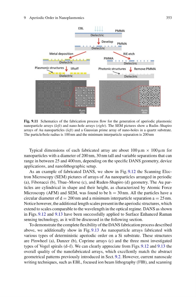
Fig. 9.11 Schematics of the fabrication process flow for the generation of aperiodic plasmonic
nanoparticle arrays (left) and nano-hole arrays (right). The SEM pictures show a Rudin–Shapiro
arrays of Au nanoparticles (left) and a Gaussian prime array of nano-holes in a quartz substrate.
The particle/hole radius is 100 nm and the minimum interparticle separation is 200 nm
Typical dimensions of each fabricated array are about 100 μm × 100 μm for
nanoparticles with a diameter of 200 nm, 30 nm tall and variable separations that can
range in between 25 and 400 nm, depending on the specific DANS geometry, device
applications, and nanolithographic setup.
As an example of fabricated DANS, we show in Fig. 9.12 the Scanning Electron Microscopy (SEM) pictures of arrays of Au nanoparticles arranged in periodic
(a), Fibonacci (b), Thue–Morse (c), and Ruden-Shapiro (d) geometry. The Au particles are cylindrical in shape and their height, as characterized by Atomic Force
Microscopy (AFM) and SEM, was found to be h = 30 nm. All the particles have a
circular diameter of d = 200 nm and a minimum interparticle separation a = 25 nm.
Notice however, the additional length scales present in the aperiodic structures, which
extend to scales comparable to the wavelength in the optical regime. DANS as shown
in Figs. 9.12 and 9.13 have been successfully applied to Surface Enhanced Raman
sensing technology, as it will be discussed in the following section.
To demonstrate the complete flexibility of the DANS fabrication process described
above, we additionally show in Fig. 9.13 Au nanoparticle arrays fabricated with
various types of deterministic aperiodic order on a Si substrate. These structures
are Pinwheel (a), Danzer (b), Coprime arrays (c) and the three most investigated
types of Vogel spirals (d–f). We can clearly appreciate from Figs. 9.12 and 9.13 the
overall quality of the nanofabricated arrays, which excellently match the abstract
geometrical patterns previously introduced in Sect. 9.2. However, current nanoscale
writing techniques, such as EBL, focused ion beam lithography (FIB), and scanning
353
Fig. 9.11 Schematics of the fabrication process flow for the generation of aperiodic plasmonic
nanoparticle arrays (left) and nano-hole arrays (right). The SEM pictures show a Rudin–Shapiro
arrays of Au nanoparticles (left) and a Gaussian prime array of nano-holes in a quartz substrate.
The particle/hole radius is 100 nm and the minimum interparticle separation is 200 nm
Typical dimensions of each fabricated array are about 100 μm × 100 μm for
nanoparticles with a diameter of 200 nm, 30 nm tall and variable separations that can
range in between 25 and 400 nm, depending on the specific DANS geometry, device
applications, and nanolithographic setup.
As an example of fabricated DANS, we show in Fig. 9.12 the Scanning Electron Microscopy (SEM) pictures of arrays of Au nanoparticles arranged in periodic
(a), Fibonacci (b), Thue–Morse (c), and Ruden-Shapiro (d) geometry. The Au particles are cylindrical in shape and their height, as characterized by Atomic Force
Microscopy (AFM) and SEM, was found to be h = 30 nm. All the particles have a
circular diameter of d = 200 nm and a minimum interparticle separation a = 25 nm.
Notice however, the additional length scales present in the aperiodic structures, which
extend to scales comparable to the wavelength in the optical regime. DANS as shown
in Figs. 9.12 and 9.13 have been successfully applied to Surface Enhanced Raman
sensing technology, as it will be discussed in the following section.
To demonstrate the complete flexibility of the DANS fabrication process described
above, we additionally show in Fig. 9.13 Au nanoparticle arrays fabricated with
various types of deterministic aperiodic order on a Si substrate. These structures
are Pinwheel (a), Danzer (b), Coprime arrays (c) and the three most investigated
types of Vogel spirals (d–f). We can clearly appreciate from Figs. 9.12 and 9.13 the
overall quality of the nanofabricated arrays, which excellently match the abstract
geometrical patterns previously introduced in Sect. 9.2. However, current nanoscale
writing techniques, such as EBL, focused ion beam lithography (FIB), and scanning