

136
M. B. Ross et al.
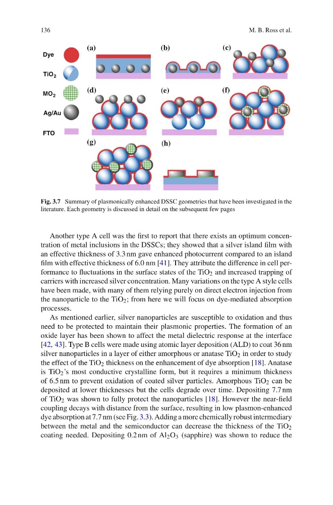
Dye
TiO 2
FTO
MO 2
Ag/Au
(a)
(b)
(c)
(d)
(e)
(f)
(g)
(h)
Fig. 3.7 Summary of plasmonically enhanced DSSC geometries that have been investigated in the
literature. Each geometry is discussed in detail on the subsequent few pages
Another type A cell was the first to report that there exists an optimum concentration of metal inclusions in the DSSCs; they showed that a silver island film with
an effective thickness of 3.3 nm gave enhanced photocurrent compared to an island
film with effective thickness of 6.0 nm [41]. They attribute the difference in cell performance to fluctuations in the surface states of the TiO 2 and increased trapping of
carriers with increased silver concentration. Many variations on the type A style cells
have been made, with many of them relying purely on direct electron injection from
the nanoparticle to the TiO 2 ; from here we will focus on dye-mediated absorption
processes.
As mentioned earlier, silver nanoparticles are susceptible to oxidation and thus
need to be protected to maintain their plasmonic properties. The formation of an
oxide layer has been shown to affect the metal dielectric response at the interface
[42, 43]. Type B cells were made using atomic layer deposition (ALD) to coat 36 nm
silver nanoparticles in a layer of either amorphous or anatase TiO 2 in order to study
the effect of the TiO 2 thickness on the enhancement of dye absorption [18]. Anatase
is TiO 2 ’s most conductive crystalline form, but it requires a minimum thickness
of 6.5 nm to prevent oxidation of coated silver particles. Amorphous TiO 2 can be
deposited at lower thicknesses but the cells degrade over time. Depositing 7.7 nm
of TiO 2 was shown to fully protect the nanoparticles [18]. However the near-field
coupling decays with distance from the surface, resulting in low plasmon-enhanced
dye absorption at 7.7 nm (see Fig. 3.3). Adding a more chemically robust intermediary
between the metal and the semiconductor can decrease the thickness of the TiO 2
coating needed. Depositing 0.2 nm of Al 2 O 3 (sapphire) was shown to reduce the
M. B. Ross et al.
Dye
TiO 2
FTO
MO 2
Ag/Au
(a)
(b)
(c)
(d)
(e)
(f)
(g)
(h)
Fig. 3.7 Summary of plasmonically enhanced DSSC geometries that have been investigated in the
literature. Each geometry is discussed in detail on the subsequent few pages
Another type A cell was the first to report that there exists an optimum concentration of metal inclusions in the DSSCs; they showed that a silver island film with
an effective thickness of 3.3 nm gave enhanced photocurrent compared to an island
film with effective thickness of 6.0 nm [41]. They attribute the difference in cell performance to fluctuations in the surface states of the TiO 2 and increased trapping of
carriers with increased silver concentration. Many variations on the type A style cells
have been made, with many of them relying purely on direct electron injection from
the nanoparticle to the TiO 2 ; from here we will focus on dye-mediated absorption
processes.
As mentioned earlier, silver nanoparticles are susceptible to oxidation and thus
need to be protected to maintain their plasmonic properties. The formation of an
oxide layer has been shown to affect the metal dielectric response at the interface
[42, 43]. Type B cells were made using atomic layer deposition (ALD) to coat 36 nm
silver nanoparticles in a layer of either amorphous or anatase TiO 2 in order to study
the effect of the TiO 2 thickness on the enhancement of dye absorption [18]. Anatase
is TiO 2 ’s most conductive crystalline form, but it requires a minimum thickness
of 6.5 nm to prevent oxidation of coated silver particles. Amorphous TiO 2 can be
deposited at lower thicknesses but the cells degrade over time. Depositing 7.7 nm
of TiO 2 was shown to fully protect the nanoparticles [18]. However the near-field
coupling decays with distance from the surface, resulting in low plasmon-enhanced
dye absorption at 7.7 nm (see Fig. 3.3). Adding a more chemically robust intermediary
between the metal and the semiconductor can decrease the thickness of the TiO 2
coating needed. Depositing 0.2 nm of Al 2 O 3 (sapphire) was shown to reduce the