

electronic changes, I-z spectroscopy, STS spectroscopy) and the possibility to
modify parameters not accessible by any other technique (e.g. by variation of the
tunnelling distance). The STM tip can be also effectively used as an active electrode
inducing electrochemical redox reactions at the surface of the solid electrolyte.
Based on this new approach the reaction kinetics of several materials such as
RbAg 4 I 5 , Ag 2 S, Cu 2 S, TaO 2 , HfO 2 and TiO 2 has been studied [21, 29–32].
4.1 Theoretical Considerations
4.1.1 Imaging and Electrochemical Reactions
On a first place STM can be used to image the surface of the solid film and precisely
(with atomic resolution) select the position for applying voltage and studying
particular process(es).
For studies on macroscopic samples, the evaluated properties of surfaces are
averaged and the main efforts are focused on the preparation of an ideal, defect free
surface. Even mono-crystalline surfaces are showing microscopic defects, possible
dislocations, missing atoms, monoatomic steps, etc., being energetically not equivalent, thus predetermining different local reaction kinetics. In that sense, STM is
providing the unique opportunity to find and select defect-free position or particular
defect site and perform locally electrochemical studies on it, without influencing
and/or gathering information from neighbouring domains.
The sensitivity of the STM towards surface morphology inhomogeneity allows to
follow the formation and dissolution of small number of atoms (even single atoms),
providing an important advantage to observe finest changes induced at the surface.
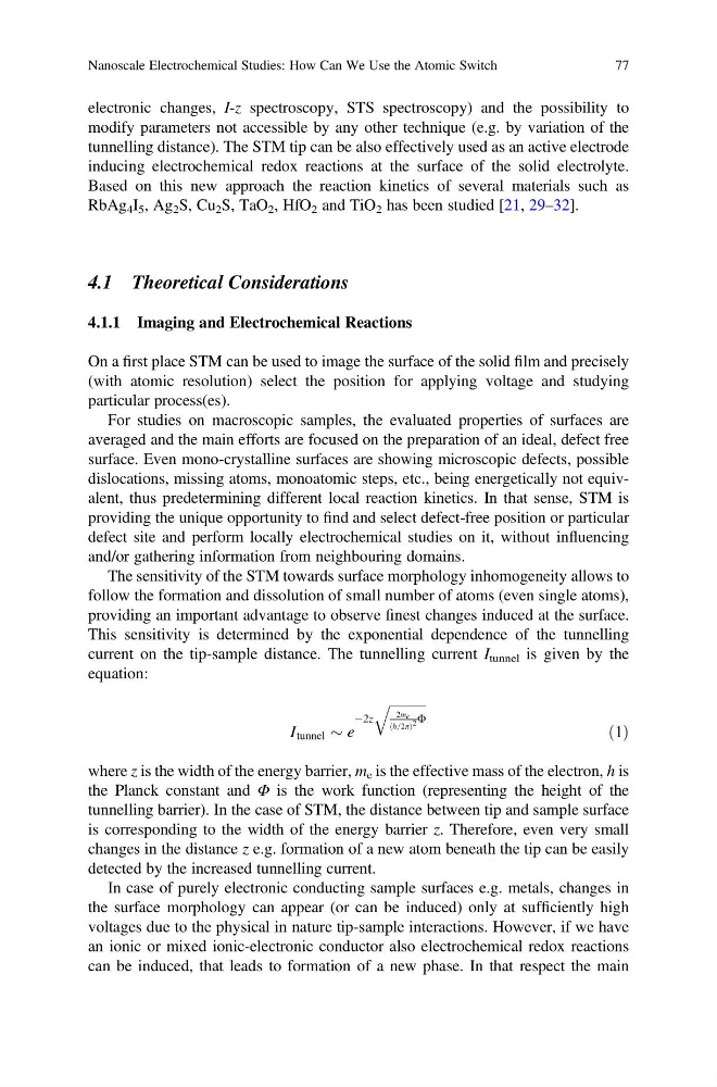
This sensitivity is determined by the exponential dependence of the tunnelling
current on the tip-sample distance. The tunnelling current I tunnel is given by the
equation:
I tunnel $ e
À2z
ffiffiffiffiffiffiffiffiffiffiffi
2me
h=2π
ð
Þ 2 Φ
q
ð1Þ
where z is the width of the energy barrier, m e is the effective mass of the electron, h is
the Planck constant and Φ is the work function (representing the height of the
tunnelling barrier). In the case of STM, the distance between tip and sample surface
is corresponding to the width of the energy barrier z. Therefore, even very small
changes in the distance z e.g. formation of a new atom beneath the tip can be easily
detected by the increased tunnelling current.
In case of purely electronic conducting sample surfaces e.g. metals, changes in
the surface morphology can appear (or can be induced) only at sufficiently high
voltages due to the physical in nature tip-sample interactions. However, if we have
an ionic or mixed ionic-electronic conductor also electrochemical redox reactions
can be induced, that leads to formation of a new phase. In that respect the main
Nanoscale Electrochemical Studies: How Can We Use the Atomic Switch
77
modify parameters not accessible by any other technique (e.g. by variation of the
tunnelling distance). The STM tip can be also effectively used as an active electrode
inducing electrochemical redox reactions at the surface of the solid electrolyte.
Based on this new approach the reaction kinetics of several materials such as
RbAg 4 I 5 , Ag 2 S, Cu 2 S, TaO 2 , HfO 2 and TiO 2 has been studied [21, 29–32].
4.1 Theoretical Considerations
4.1.1 Imaging and Electrochemical Reactions
On a first place STM can be used to image the surface of the solid film and precisely
(with atomic resolution) select the position for applying voltage and studying
particular process(es).
For studies on macroscopic samples, the evaluated properties of surfaces are
averaged and the main efforts are focused on the preparation of an ideal, defect free
surface. Even mono-crystalline surfaces are showing microscopic defects, possible
dislocations, missing atoms, monoatomic steps, etc., being energetically not equivalent, thus predetermining different local reaction kinetics. In that sense, STM is
providing the unique opportunity to find and select defect-free position or particular
defect site and perform locally electrochemical studies on it, without influencing
and/or gathering information from neighbouring domains.
The sensitivity of the STM towards surface morphology inhomogeneity allows to
follow the formation and dissolution of small number of atoms (even single atoms),
providing an important advantage to observe finest changes induced at the surface.
This sensitivity is determined by the exponential dependence of the tunnelling
current on the tip-sample distance. The tunnelling current I tunnel is given by the
equation:
I tunnel $ e
À2z
ffiffiffiffiffiffiffiffiffiffiffi
2me
h=2π
ð
Þ 2 Φ
q
ð1Þ
where z is the width of the energy barrier, m e is the effective mass of the electron, h is
the Planck constant and Φ is the work function (representing the height of the
tunnelling barrier). In the case of STM, the distance between tip and sample surface
is corresponding to the width of the energy barrier z. Therefore, even very small
changes in the distance z e.g. formation of a new atom beneath the tip can be easily
detected by the increased tunnelling current.
In case of purely electronic conducting sample surfaces e.g. metals, changes in
the surface morphology can appear (or can be induced) only at sufficiently high
voltages due to the physical in nature tip-sample interactions. However, if we have
an ionic or mixed ionic-electronic conductor also electrochemical redox reactions
can be induced, that leads to formation of a new phase. In that respect the main
Nanoscale Electrochemical Studies: How Can We Use the Atomic Switch
77