

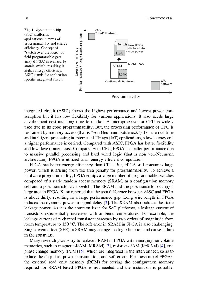
integrated circuit (ASIC) shows the highest performance and lowest power consumption but it has low flexibility for various applications. It also needs large
development cost and long time to market. A microprocessor or CPU is widely
used due to its good programmability. But, the processing performance of CPU is
restrained by memory access (that is “von Neumann bottleneck”). For the real time
and intelligent processing in Internet-of-Things (IoT) applications, a low latency and
a higher performance is desired. Compared with ASIC, FPGA has better flexibility
and low development cost. Compared with CPU, FPGA has better performance due
to massive parallel processing and hard wired logic (that is non von-Neumann
architecture). FPGA is utilized as an energy-efficient computation.
FPGA has better energy efficiency than CPU. But, FPGA still consumes large
power, which is arising from the area penalty for programmability. To achieve a
hardware programmability, FPGA equips a large number of programmable switches
composed of a static random access memory (SRAM) as a configuration memory
cell and a pass transistor as a switch. The SRAM and the pass transistor occupy a
large area in FPGA. Kuon reported that the area difference between AISC and FPGA
is about thirty, resulting in a large performance gap. Long wire length in FPGA
induces the dynamic power or signal delay [2]. The SRAM also induces the static
leakage power. As it is the common issue for SoC platforms, a leakage current of
transistors exponentially increases with ambient temperatures. For example, the
leakage current of n-channel transistor increases by two orders of magnitude from
room temperature to 150
C. The soft error in SRAM in FPGA is also challenging.
Single event effect (SEE) in SRAM may change the logic function and cause failure
in the apparatus.
Many research groups try to replace SRAM in FPGA with emerging nonvolatile
memories, such as magnetic-RAM (MRAM) [3], resistive-RAM (ReRAM) [4], and
phase change memory (PCM) [5], which are integrated in the interconnect, so as to
reduce the chip size, power consumption, and soft errors. For these novel FPGAs,
the external read only memory (ROM) for storing the configuration memory
required for SRAM-based FPGA is not needed and the instant-on is possible.
SRAM-FPGA
ASIC
“Hard” Hardware
Programmability
CPU
Software
Logic
SRAM
Logic
Switch Novel FPGA
-Reduced size
-Low power
Configurable Hardware
y
c
n
e
i
c
i
f
f
e
y
g
r
e
n
E
n
o
i
t
p
m
u
s
n
o
c
y
g
r
e
n
E
/
e
c
n
a
m
r
o
f
r
e
P
Fig. 1 System-on-Chip
(SoC) platforms
applications in terms of
programmability and energy
efficiency. Concept of
“switch over the logic” of
field programmable gate
array (FPGA) is realized by
atomic switch, resulting in
higher energy efficiency.
ASIC stands for application
specific integrated circuit
18
T. Sakamoto et al.
development cost and long time to market. A microprocessor or CPU is widely
used due to its good programmability. But, the processing performance of CPU is
restrained by memory access (that is “von Neumann bottleneck”). For the real time
and intelligent processing in Internet-of-Things (IoT) applications, a low latency and
a higher performance is desired. Compared with ASIC, FPGA has better flexibility
and low development cost. Compared with CPU, FPGA has better performance due
to massive parallel processing and hard wired logic (that is non von-Neumann
architecture). FPGA is utilized as an energy-efficient computation.
FPGA has better energy efficiency than CPU. But, FPGA still consumes large
power, which is arising from the area penalty for programmability. To achieve a
hardware programmability, FPGA equips a large number of programmable switches
composed of a static random access memory (SRAM) as a configuration memory
cell and a pass transistor as a switch. The SRAM and the pass transistor occupy a
large area in FPGA. Kuon reported that the area difference between AISC and FPGA
is about thirty, resulting in a large performance gap. Long wire length in FPGA
induces the dynamic power or signal delay [2]. The SRAM also induces the static
leakage power. As it is the common issue for SoC platforms, a leakage current of
transistors exponentially increases with ambient temperatures. For example, the
leakage current of n-channel transistor increases by two orders of magnitude from
room temperature to 150
C. The soft error in SRAM in FPGA is also challenging.
Single event effect (SEE) in SRAM may change the logic function and cause failure
in the apparatus.
Many research groups try to replace SRAM in FPGA with emerging nonvolatile
memories, such as magnetic-RAM (MRAM) [3], resistive-RAM (ReRAM) [4], and
phase change memory (PCM) [5], which are integrated in the interconnect, so as to
reduce the chip size, power consumption, and soft errors. For these novel FPGAs,
the external read only memory (ROM) for storing the configuration memory
required for SRAM-based FPGA is not needed and the instant-on is possible.
SRAM-FPGA
ASIC
“Hard” Hardware
Programmability
CPU
Software
Logic
SRAM
Logic
Switch Novel FPGA
-Reduced size
-Low power
Configurable Hardware
y
c
n
e
i
c
i
f
f
e
y
g
r
e
n
E
n
o
i
t
p
m
u
s
n
o
c
y
g
r
e
n
E
/
e
c
n
a
m
r
o
f
r
e
P
Fig. 1 System-on-Chip
(SoC) platforms
applications in terms of
programmability and energy
efficiency. Concept of
“switch over the logic” of
field programmable gate
array (FPGA) is realized by
atomic switch, resulting in
higher energy efficiency.
ASIC stands for application
specific integrated circuit
18
T. Sakamoto et al.