

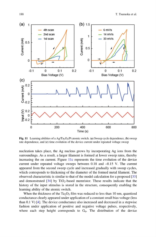
nucleation takes place, the Ag nucleus grows by incorporating Ag ions from the
surroundings. As a result, a larger filament is formed at lower sweep rates, thereby
increasing the on current. Figure 11c represents the time evolution of the device
current under repeated voltage sweeps between 0.18 and –0.15 V. The current
appeared from the second sweep cycle and increased gradually with sweep cycles,
which corresponds to thickening of the diameter of the formed metal filament. The
observed characteristic is similar to that of the model calculation for a proposed [33]
and demonstrated [34] by TiO 2 -based memristor. These results indicate that the
history of the input stimulus is stored in the structure, consequently enabling the
learning ability of the atomic switch.
When the thickness of the Ta 2 O 5 film was reduced to less than 10 nm, quantized
conductance clearly appeared under application of a constant small bias voltage (less
than 0.1 V) [4]. The device conductance also increased and decreased in a stepwise
fashion under application of positive and negative voltage pulses, respectively,
where each step height corresponds to G 0 . The distribution of the device
Fig. 11 Learning abilities of a Ag/Ta 2 O 5 /Pt atomic switch. (a) Sweep cycle dependence, (b) sweep
rate dependence, and (c) time evolution of the device current under repeated voltage sweep
188
T. Tsuruoka et al.
surroundings. As a result, a larger filament is formed at lower sweep rates, thereby
increasing the on current. Figure 11c represents the time evolution of the device
current under repeated voltage sweeps between 0.18 and –0.15 V. The current
appeared from the second sweep cycle and increased gradually with sweep cycles,
which corresponds to thickening of the diameter of the formed metal filament. The
observed characteristic is similar to that of the model calculation for a proposed [33]
and demonstrated [34] by TiO 2 -based memristor. These results indicate that the
history of the input stimulus is stored in the structure, consequently enabling the
learning ability of the atomic switch.
When the thickness of the Ta 2 O 5 film was reduced to less than 10 nm, quantized
conductance clearly appeared under application of a constant small bias voltage (less
than 0.1 V) [4]. The device conductance also increased and decreased in a stepwise
fashion under application of positive and negative voltage pulses, respectively,
where each step height corresponds to G 0 . The distribution of the device
Fig. 11 Learning abilities of a Ag/Ta 2 O 5 /Pt atomic switch. (a) Sweep cycle dependence, (b) sweep
rate dependence, and (c) time evolution of the device current under repeated voltage sweep
188
T. Tsuruoka et al.