

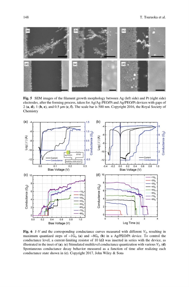
Fig. 5 SEM images of the filament growth morphology between Ag (left side) and Pt (right side)
electrodes, after the forming process, taken for Ag/Ag-PEO/Pt and Ag/PEO/Pt devices with gaps of
2 (a, d), 1 (b, e), and 0.5 μm (c, f). The scale bar is 500 nm. Copyright 2016, the Royal Society of
Chemistry
Fig. 6 I–V and the corresponding conductance curves measured with different V S , resulting in
maximum quantized steps of ~1G 0 (a) and ~8G 0 (b) in a Ag/PEO/Pt device. To control the
conductance level, a current-limiting resistor of 10 kΩ was inserted in series with the device, as
illustrated in the inset of (a). (c) Stimulated multilevel conductance quantization with various V S . (d)
Spontaneous conductance decay behavior measured as a function of time after realizing each
conductance state shown in (c). Copyright 2017, John Wiley & Sons
148
T. Tsuruoka et al.
electrodes, after the forming process, taken for Ag/Ag-PEO/Pt and Ag/PEO/Pt devices with gaps of
2 (a, d), 1 (b, e), and 0.5 μm (c, f). The scale bar is 500 nm. Copyright 2016, the Royal Society of
Chemistry
Fig. 6 I–V and the corresponding conductance curves measured with different V S , resulting in
maximum quantized steps of ~1G 0 (a) and ~8G 0 (b) in a Ag/PEO/Pt device. To control the
conductance level, a current-limiting resistor of 10 kΩ was inserted in series with the device, as
illustrated in the inset of (a). (c) Stimulated multilevel conductance quantization with various V S . (d)
Spontaneous conductance decay behavior measured as a function of time after realizing each
conductance state shown in (c). Copyright 2017, John Wiley & Sons
148
T. Tsuruoka et al.