

of semiconductor transistors. If a revolutionary novel switch device is developed, it
will be possible to innovatively advance information and communication equipment.
Our development of innovative atomic switches, whose operating principles are
completely different from that of the semiconductor transistor, are due to the
discovery of unexpected solid electrochemical nanophenomenon, namely by serendipity [1–4]. In our initial research, we were developing nanotechnology to deposit
metal atoms one by one on a substrate, by utilizing metal ion migration within the
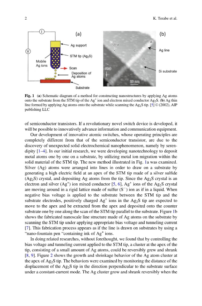
solid material of the STM tip. The new method illustrated in Fig. 1a was examined.
Silver (Ag) atoms were arranged into lines in order to draw on a substrate by
generating a high electric field at an apex of the STM tip made of a silver sulfide
(Ag 2 S) crystal, and depositing Ag atoms from the tip. Since the Ag 2 S crystal is an
electron and silver (Ag
+
) ion mixed conductor [5, 6], Ag
+ ions of the Ag 2 S crystal
are moving around in a rigid lattice made of sulfur (S
À
) ion as if in a liquid. When
negative bias voltage is applied to the substrate between the STM tip and the
substrate electrodes, positively charged Ag
+ ions in the Ag 2 S tip are expected to
move to the apex and be extracted from the apex and deposited onto the counter
substrate one by one along the scan of the STM tip parallel to the substrate. Figure 1b
shows the fabricated nanoscale line structure made of Ag atoms on the substrate by
scanning the STM tip under applying appropriate bias voltage and tunneling current
[7]. This fabrication process appears as if the line is drawn on substrates by using a
“nano-fountain pen “containing ink of Ag
+ ions.
In doing related researches, without forethought, we found that by controlling the
bias voltage and tunneling current applied to the STM tip, a cluster at the apex of the
tip, consisting of a small amount of Ag atoms, could be reversibly grew and shrank
[8, 9]. Figure 2 shows the growth and shrinkage behavior of the Ag atom cluster at
the apex of Ag 2 S tip. The behaviors were examined by monitoring the distance of the
displacement of the Ag 2 S tip in the direction perpendicular to the substrate surface
under a constant-current mode. The Ag cluster grow and shrank reversibly when the
Mobile
Ag ions
Ag line
Si substrate
(a)
(b)
Fig. 1 (a) Schematic diagram of a method for constructing nanostructures by applying Ag atoms
onto the substrate from the STM tip of the Ag
+ ion and electron mixed conductor Ag 2 S. (b) Ag thin
line formed by applying Ag atoms onto the substrate while scanning the Ag 2 S tip. [5] © (2002), AIP
publishing LLC
2
K. Terabe et al.
will be possible to innovatively advance information and communication equipment.
Our development of innovative atomic switches, whose operating principles are
completely different from that of the semiconductor transistor, are due to the
discovery of unexpected solid electrochemical nanophenomenon, namely by serendipity [1–4]. In our initial research, we were developing nanotechnology to deposit
metal atoms one by one on a substrate, by utilizing metal ion migration within the
solid material of the STM tip. The new method illustrated in Fig. 1a was examined.
Silver (Ag) atoms were arranged into lines in order to draw on a substrate by
generating a high electric field at an apex of the STM tip made of a silver sulfide
(Ag 2 S) crystal, and depositing Ag atoms from the tip. Since the Ag 2 S crystal is an
electron and silver (Ag
+
) ion mixed conductor [5, 6], Ag
+ ions of the Ag 2 S crystal
are moving around in a rigid lattice made of sulfur (S
À
) ion as if in a liquid. When
negative bias voltage is applied to the substrate between the STM tip and the
substrate electrodes, positively charged Ag
+ ions in the Ag 2 S tip are expected to
move to the apex and be extracted from the apex and deposited onto the counter
substrate one by one along the scan of the STM tip parallel to the substrate. Figure 1b
shows the fabricated nanoscale line structure made of Ag atoms on the substrate by
scanning the STM tip under applying appropriate bias voltage and tunneling current
[7]. This fabrication process appears as if the line is drawn on substrates by using a
“nano-fountain pen “containing ink of Ag
+ ions.
In doing related researches, without forethought, we found that by controlling the
bias voltage and tunneling current applied to the STM tip, a cluster at the apex of the
tip, consisting of a small amount of Ag atoms, could be reversibly grew and shrank
[8, 9]. Figure 2 shows the growth and shrinkage behavior of the Ag atom cluster at
the apex of Ag 2 S tip. The behaviors were examined by monitoring the distance of the
displacement of the Ag 2 S tip in the direction perpendicular to the substrate surface
under a constant-current mode. The Ag cluster grow and shrank reversibly when the
Mobile
Ag ions
Ag line
Si substrate
(a)
(b)
Fig. 1 (a) Schematic diagram of a method for constructing nanostructures by applying Ag atoms
onto the substrate from the STM tip of the Ag
+ ion and electron mixed conductor Ag 2 S. (b) Ag thin
line formed by applying Ag atoms onto the substrate while scanning the Ag 2 S tip. [5] © (2002), AIP
publishing LLC
2
K. Terabe et al.