

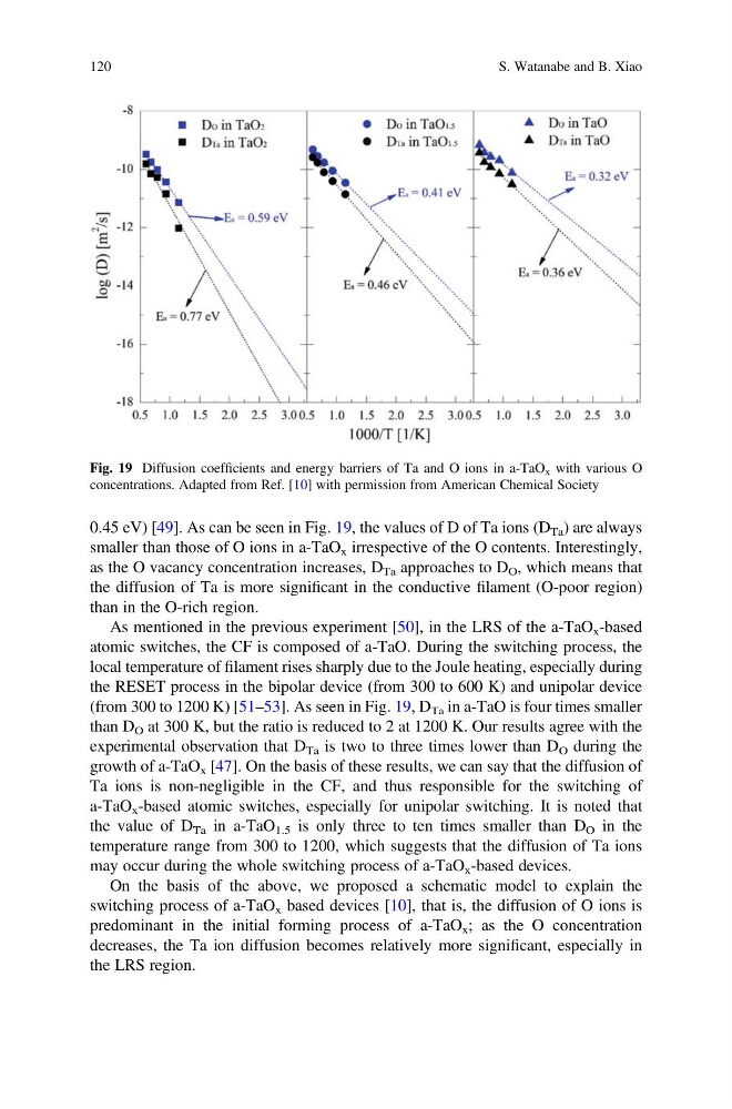
0.45 eV) [49]. As can be seen in Fig. 19, the values of D of Ta ions (D Ta ) are always
smaller than those of O ions in a-TaO x irrespective of the O contents. Interestingly,
as the O vacancy concentration increases, D Ta approaches to D O , which means that
the diffusion of Ta is more significant in the conductive filament (O-poor region)
than in the O-rich region.
As mentioned in the previous experiment [50], in the LRS of the a-TaO x -based
atomic switches, the CF is composed of a-TaO. During the switching process, the
local temperature of filament rises sharply due to the Joule heating, especially during
the RESET process in the bipolar device (from 300 to 600 K) and unipolar device
(from 300 to 1200 K) [51–53]. As seen in Fig. 19, D Ta in a-TaO is four times smaller
than D O at 300 K, but the ratio is reduced to 2 at 1200 K. Our results agree with the
experimental observation that D Ta is two to three times lower than D O during the
growth of a-TaO x [47]. On the basis of these results, we can say that the diffusion of
Ta ions is non-negligible in the CF, and thus responsible for the switching of
a-TaO x -based atomic switches, especially for unipolar switching. It is noted that
the value of D Ta in a-TaO 1.5 is only three to ten times smaller than D O in the
temperature range from 300 to 1200, which suggests that the diffusion of Ta ions
may occur during the whole switching process of a-TaO x -based devices.
On the basis of the above, we proposed a schematic model to explain the
switching process of a-TaO x based devices [10], that is, the diffusion of O ions is
predominant in the initial forming process of a-TaO x ; as the O concentration
decreases, the Ta ion diffusion becomes relatively more significant, especially in
the LRS region.
Fig. 19 Diffusion coefficients and energy barriers of Ta and O ions in a-TaO x with various O
concentrations. Adapted from Ref. [10] with permission from American Chemical Society
120
S. Watanabe and B. Xiao
smaller than those of O ions in a-TaO x irrespective of the O contents. Interestingly,
as the O vacancy concentration increases, D Ta approaches to D O , which means that
the diffusion of Ta is more significant in the conductive filament (O-poor region)
than in the O-rich region.
As mentioned in the previous experiment [50], in the LRS of the a-TaO x -based
atomic switches, the CF is composed of a-TaO. During the switching process, the
local temperature of filament rises sharply due to the Joule heating, especially during
the RESET process in the bipolar device (from 300 to 600 K) and unipolar device
(from 300 to 1200 K) [51–53]. As seen in Fig. 19, D Ta in a-TaO is four times smaller
than D O at 300 K, but the ratio is reduced to 2 at 1200 K. Our results agree with the
experimental observation that D Ta is two to three times lower than D O during the
growth of a-TaO x [47]. On the basis of these results, we can say that the diffusion of
Ta ions is non-negligible in the CF, and thus responsible for the switching of
a-TaO x -based atomic switches, especially for unipolar switching. It is noted that
the value of D Ta in a-TaO 1.5 is only three to ten times smaller than D O in the
temperature range from 300 to 1200, which suggests that the diffusion of Ta ions
may occur during the whole switching process of a-TaO x -based devices.
On the basis of the above, we proposed a schematic model to explain the
switching process of a-TaO x based devices [10], that is, the diffusion of O ions is
predominant in the initial forming process of a-TaO x ; as the O concentration
decreases, the Ta ion diffusion becomes relatively more significant, especially in
the LRS region.
Fig. 19 Diffusion coefficients and energy barriers of Ta and O ions in a-TaO x with various O
concentrations. Adapted from Ref. [10] with permission from American Chemical Society
120
S. Watanabe and B. Xiao