

6 Bio-microelectromechanical Systems (BioMEMS) …
139
was deposited to protect the chip. Via RIE, the contact pads were opened and the
chips were diced. The chip was wire-bonded and mounted to a printed circuit board.
Soft lithography was performed to fabricate the microfluidic structures.
The microchannels molds were fabricated by SU-8 on silicon. First, an aluminum
physical mask was fabricated by sputtering aluminum on a quartz substrate and
patterning it via wet etching. SU-8 resist was spin-coated and exposed to the UV
light through the aluminum mask then baked and developed in propylene glycol
methyl ether acetate (PGMEA). A second flat PDMS layer was created on top of a
silicon wafer by spin coating and cured. Afterwards, the pieces were detached from
the molds. A corona discharge was used to oxidize the flat 500 m thick PDMS pieces
and the surface of the PDMS piece with the defined microchannels, which were then
put in contact and left to seal irreversibly.
Two micromachined PMMA plates were aligned and held the microfluidic device
on top of the wire bonded photodiode chip to accommodate the integration of the
photodiode array and the microfluidic network. The PDMS microchannel piece was
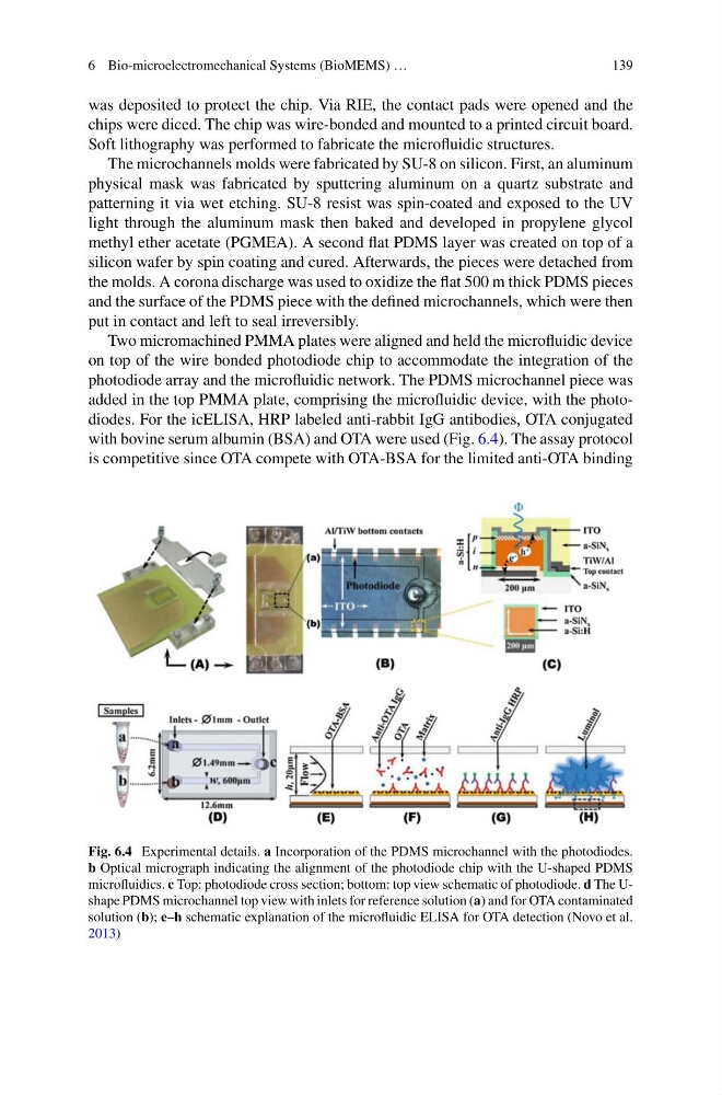
added in the top PMMA plate, comprising the microfluidic device, with the photodiodes. For the icELISA, HRP labeled anti-rabbit IgG antibodies, OTA conjugated
with bovine serum albumin (BSA) and OTA were used (Fig. 6.4). The assay protocol
is competitive since OTA compete with OTA-BSA for the limited anti-OTA binding
Fig. 6.4 Experimental details. a Incorporation of the PDMS microchannel with the photodiodes.
b Optical micrograph indicating the alignment of the photodiode chip with the U-shaped PDMS
microfluidics. c Top: photodiode cross section; bottom: top view schematic of photodiode. d The Ushape PDMS microchannel top view with inlets for reference solution (a) and for OTA contaminated
solution (b); e–h schematic explanation of the microfluidic ELISA for OTA detection (Novo et al.
2013)
139
was deposited to protect the chip. Via RIE, the contact pads were opened and the
chips were diced. The chip was wire-bonded and mounted to a printed circuit board.
Soft lithography was performed to fabricate the microfluidic structures.
The microchannels molds were fabricated by SU-8 on silicon. First, an aluminum
physical mask was fabricated by sputtering aluminum on a quartz substrate and
patterning it via wet etching. SU-8 resist was spin-coated and exposed to the UV
light through the aluminum mask then baked and developed in propylene glycol
methyl ether acetate (PGMEA). A second flat PDMS layer was created on top of a
silicon wafer by spin coating and cured. Afterwards, the pieces were detached from
the molds. A corona discharge was used to oxidize the flat 500 m thick PDMS pieces
and the surface of the PDMS piece with the defined microchannels, which were then
put in contact and left to seal irreversibly.
Two micromachined PMMA plates were aligned and held the microfluidic device
on top of the wire bonded photodiode chip to accommodate the integration of the
photodiode array and the microfluidic network. The PDMS microchannel piece was
added in the top PMMA plate, comprising the microfluidic device, with the photodiodes. For the icELISA, HRP labeled anti-rabbit IgG antibodies, OTA conjugated
with bovine serum albumin (BSA) and OTA were used (Fig. 6.4). The assay protocol
is competitive since OTA compete with OTA-BSA for the limited anti-OTA binding
Fig. 6.4 Experimental details. a Incorporation of the PDMS microchannel with the photodiodes.
b Optical micrograph indicating the alignment of the photodiode chip with the U-shaped PDMS
microfluidics. c Top: photodiode cross section; bottom: top view schematic of photodiode. d The Ushape PDMS microchannel top view with inlets for reference solution (a) and for OTA contaminated
solution (b); e–h schematic explanation of the microfluidic ELISA for OTA detection (Novo et al.
2013)