

17 Interconnect Quality and Reliability of 3D Packaging
561
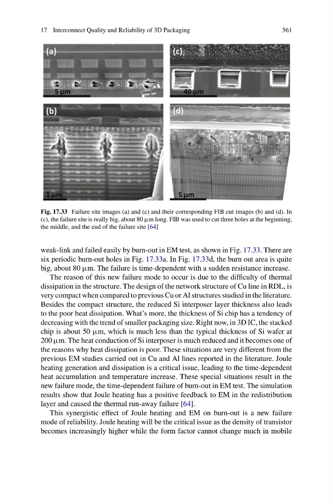
Fig. 17.33 Failure site images (a) and (c) and their corresponding FIB cut images (b) and (d). In
(c), the failure site is really big, about 80 μm long. FIB was used to cut three holes at the beginning,
the middle, and the end of the failure site [64]
weak-link and failed easily by burn-out in EM test, as shown in Fig. 17.33. There are
six periodic burn-out holes in Fig. 17.33a. In Fig. 17.33d, the burn out area is quite
big, about 80 μm. The failure is time-dependent with a sudden resistance increase.
The reason of this new failure mode to occur is due to the difficulty of thermal
dissipation in the structure. The design of the network structure of Cu line in RDL, is
very compact when compared to previous Cu or Al structures studied in the literature.
Besides the compact structure, the reduced Si interposer layer thickness also leads
to the poor heat dissipation. What’s more, the thickness of Si chip has a tendency of
decreasing with the trend of smaller packaging size. Right now, in 3D IC, the stacked
chip is about 50 μm, which is much less than the typical thickness of Si wafer at
200 μm. The heat conduction of Si interposer is much reduced and it becomes one of
the reasons why heat dissipation is poor. These situations are very different from the
previous EM studies carried out in Cu and Al lines reported in the literature. Joule
heating generation and dissipation is a critical issue, leading to the time-dependent
heat accumulation and temperature increase. These special situations result in the
new failure mode, the time-dependent failure of burn-out in EM test. The simulation
results show that Joule heating has a positive feedback to EM in the redistribution
layer and caused the thermal run-away failure [64].
This synergistic effect of Joule heating and EM on burn-out is a new failure
mode of reliability. Joule heating will be the critical issue as the density of transistor
becomes increasingly higher while the form factor cannot change much in mobile
561
Fig. 17.33 Failure site images (a) and (c) and their corresponding FIB cut images (b) and (d). In
(c), the failure site is really big, about 80 μm long. FIB was used to cut three holes at the beginning,
the middle, and the end of the failure site [64]
weak-link and failed easily by burn-out in EM test, as shown in Fig. 17.33. There are
six periodic burn-out holes in Fig. 17.33a. In Fig. 17.33d, the burn out area is quite
big, about 80 μm. The failure is time-dependent with a sudden resistance increase.
The reason of this new failure mode to occur is due to the difficulty of thermal
dissipation in the structure. The design of the network structure of Cu line in RDL, is
very compact when compared to previous Cu or Al structures studied in the literature.
Besides the compact structure, the reduced Si interposer layer thickness also leads
to the poor heat dissipation. What’s more, the thickness of Si chip has a tendency of
decreasing with the trend of smaller packaging size. Right now, in 3D IC, the stacked
chip is about 50 μm, which is much less than the typical thickness of Si wafer at
200 μm. The heat conduction of Si interposer is much reduced and it becomes one of
the reasons why heat dissipation is poor. These situations are very different from the
previous EM studies carried out in Cu and Al lines reported in the literature. Joule
heating generation and dissipation is a critical issue, leading to the time-dependent
heat accumulation and temperature increase. These special situations result in the
new failure mode, the time-dependent failure of burn-out in EM test. The simulation
results show that Joule heating has a positive feedback to EM in the redistribution
layer and caused the thermal run-away failure [64].
This synergistic effect of Joule heating and EM on burn-out is a new failure
mode of reliability. Joule heating will be the critical issue as the density of transistor
becomes increasingly higher while the form factor cannot change much in mobile