

492
P. Vianco and M. Neilsen
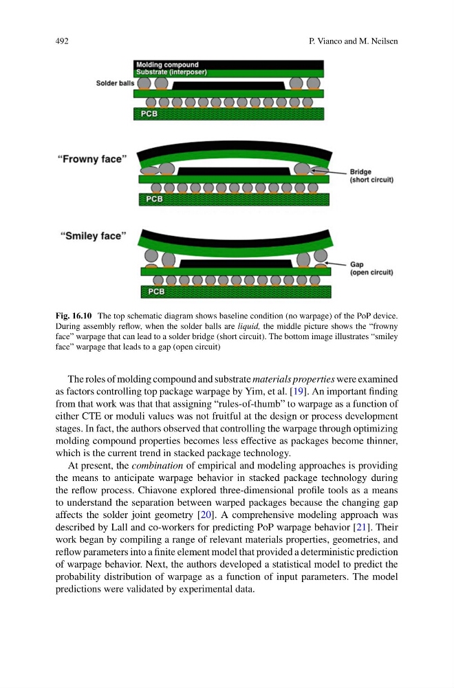
Fig. 16.10 The top schematic diagram shows baseline condition (no warpage) of the PoP device.
During assembly reflow, when the solder balls are liquid, the middle picture shows the “frowny
face” warpage that can lead to a solder bridge (short circuit). The bottom image illustrates “smiley
face” warpage that leads to a gap (open circuit)
The roles of molding compound and substrate materials properties were examined
as factors controlling top package warpage by Yim, et al. [19]. An important finding
from that work was that that assigning “rules-of-thumb” to warpage as a function of
either CTE or moduli values was not fruitful at the design or process development
stages. In fact, the authors observed that controlling the warpage through optimizing
molding compound properties becomes less effective as packages become thinner,
which is the current trend in stacked package technology.
At present, the combination of empirical and modeling approaches is providing
the means to anticipate warpage behavior in stacked package technology during
the reflow process. Chiavone explored three-dimensional profile tools as a means
to understand the separation between warped packages because the changing gap
affects the solder joint geometry [20]. A comprehensive modeling approach was
described by Lall and co-workers for predicting PoP warpage behavior [21]. Their
work began by compiling a range of relevant materials properties, geometries, and
reflow parameters into a finite element model that provided a deterministic prediction
of warpage behavior. Next, the authors developed a statistical model to predict the
probability distribution of warpage as a function of input parameters. The model
predictions were validated by experimental data.
P. Vianco and M. Neilsen
Fig. 16.10 The top schematic diagram shows baseline condition (no warpage) of the PoP device.
During assembly reflow, when the solder balls are liquid, the middle picture shows the “frowny
face” warpage that can lead to a solder bridge (short circuit). The bottom image illustrates “smiley
face” warpage that leads to a gap (open circuit)
The roles of molding compound and substrate materials properties were examined
as factors controlling top package warpage by Yim, et al. [19]. An important finding
from that work was that that assigning “rules-of-thumb” to warpage as a function of
either CTE or moduli values was not fruitful at the design or process development
stages. In fact, the authors observed that controlling the warpage through optimizing
molding compound properties becomes less effective as packages become thinner,
which is the current trend in stacked package technology.
At present, the combination of empirical and modeling approaches is providing
the means to anticipate warpage behavior in stacked package technology during
the reflow process. Chiavone explored three-dimensional profile tools as a means
to understand the separation between warped packages because the changing gap
affects the solder joint geometry [20]. A comprehensive modeling approach was
described by Lall and co-workers for predicting PoP warpage behavior [21]. Their
work began by compiling a range of relevant materials properties, geometries, and
reflow parameters into a finite element model that provided a deterministic prediction
of warpage behavior. Next, the authors developed a statistical model to predict the
probability distribution of warpage as a function of input parameters. The model
predictions were validated by experimental data.