

488
P. Vianco and M. Neilsen
compounds), PCB, and the solder joints. Attention should also be given to the glass
transition temperature (T g ) of the underfill material and the abrupt change in materials
properties associated with crossing it during a temperature ramp. Although it is not
possible to avoid the glass transition point during the reflow process, it is preferred
to avoid T g during accelerated aging and/or in-service condition to minimize solder
joint degradation. The wide variety of underfill materials on the market, today, allows
design and process engineers the opportunity to optimize this technology over a range
of performance and reliability requirements.
The second step is to determine those stacked package gaps that require an underfill
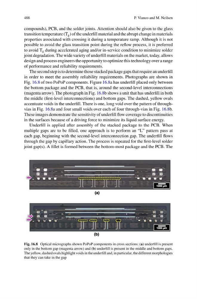
in order to meet the assembly reliability requirements. Photographs are shown in
Fig. 16.8 of two PoPoP components. Figure 16.8a has underfill placed only between
the bottom package and the PCB, that is, around the second-level interconnections
(magenta arrow). The photograph in Fig. 16.8b shows a unit that has underfill in both
the middle (first-level interconnections) and bottom gaps. The dashed, yellow ovals
accentuate voids in the underfill. There is one, long void over the pattern of throughvias in Fig. 16.8a and four small voids over each of four through-vias in Fig. 16.8b.
These images demonstrate the sensitivity of underfill flow coverage to discontinuities
in the surfaces because of a driving force to minimize its liquid surface energy.
Underfill is applied after assembly of the stacked package to the PCB. When
multiple gaps are to be filled, one approach is to perform an “L” pattern pass at
each gap, beginning with the second-level interconnection gap. The underfill flows
through the gap by capillary action. The process is repeated for the first-level solder
joint gap(s). A fillet is formed between the bottom-most package and the PCB. The
Fig. 16.8 Optical micrographs shown PoPoP components in cross sections: (a) underfill is present
only in the bottom gap (magenta arrow) and (b) underfill is present in the middle and bottom gaps.
The yellow, dashed ovals highlight voids in the underfill and, in particular, the different morphologies
that they can take in the gap
P. Vianco and M. Neilsen
compounds), PCB, and the solder joints. Attention should also be given to the glass
transition temperature (T g ) of the underfill material and the abrupt change in materials
properties associated with crossing it during a temperature ramp. Although it is not
possible to avoid the glass transition point during the reflow process, it is preferred
to avoid T g during accelerated aging and/or in-service condition to minimize solder
joint degradation. The wide variety of underfill materials on the market, today, allows
design and process engineers the opportunity to optimize this technology over a range
of performance and reliability requirements.
The second step is to determine those stacked package gaps that require an underfill
in order to meet the assembly reliability requirements. Photographs are shown in
Fig. 16.8 of two PoPoP components. Figure 16.8a has underfill placed only between
the bottom package and the PCB, that is, around the second-level interconnections
(magenta arrow). The photograph in Fig. 16.8b shows a unit that has underfill in both
the middle (first-level interconnections) and bottom gaps. The dashed, yellow ovals
accentuate voids in the underfill. There is one, long void over the pattern of throughvias in Fig. 16.8a and four small voids over each of four through-vias in Fig. 16.8b.
These images demonstrate the sensitivity of underfill flow coverage to discontinuities
in the surfaces because of a driving force to minimize its liquid surface energy.
Underfill is applied after assembly of the stacked package to the PCB. When
multiple gaps are to be filled, one approach is to perform an “L” pattern pass at
each gap, beginning with the second-level interconnection gap. The underfill flows
through the gap by capillary action. The process is repeated for the first-level solder
joint gap(s). A fillet is formed between the bottom-most package and the PCB. The
Fig. 16.8 Optical micrographs shown PoPoP components in cross sections: (a) underfill is present
only in the bottom gap (magenta arrow) and (b) underfill is present in the middle and bottom gaps.
The yellow, dashed ovals highlight voids in the underfill and, in particular, the different morphologies
that they can take in the gap