

15 Die and Package Level Thermal and Thermal/Moisture Stresses …
465
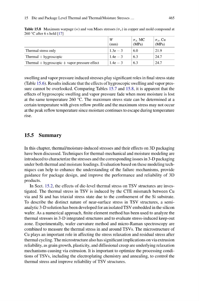
Table 15.8 Maximum warpage (w) and von Mises stresses (σ e ) in copper and mold compound at
260 °C after 6 s hold [17]
W
(mm)
σ e, MC
(MPa)
σ e , Cu
(MPa)
Thermal stress only
1.3e − 3
6.0
21.9
Thermal + hygroscopic
1.4e − 3
6.3
24.7
Thermal + hygroscopic + vapor pressure effect
1.4e − 3
6.3
24.7
swelling and vapor pressure induced stresses play significant roles in final stress state
(Table 15.6). Results indicate that the effects of hygroscopic swelling and vapor pressure cannot be overlooked. Comparing Tables 15.7 and 15.8, it is apparent that the
effects of hygroscopic swelling and vapor pressure fade when more moisture is lost
at the same temperature 260 °C. The maximum stress state can be determined at a
certain temperature with given reflow profile and the maximum stress may not occur
at the peak reflow temperature since moisture continues to escape during temperature
rise.
15.5 Summary
In this chapter, thermal/moisture-induced stresses and their effects on 3D packaging
have been discussed. Techniques for thermal-mechanical and moisture modeling are
introduced to characterize the stresses and the corresponding issues in 3-D packaging
under both thermal and moisture loadings. Evaluation based on these modeling techniques can help to enhance the understanding of the failure mechanisms, provide
guidance for package design, and improve the performance and reliability of 3D
products.
In Sect. 15.2, the effects of die-level thermal stress on TSV structures are investigated. The thermal stress in TSV is induced by the CTE mismatch between Cu
via and Si and has triaxial stress state due to the confinement of the Si substrate.
To describe the distinct nature of near-surface stress in TSV structures, a semianalytic 3-D solution has been developed for an isolated TSV embedded in the silicon
wafer. As a numerical approach, finite element method has been used to analyze the
thermal stresses in 3-D integrated structures and to evaluate stress-induced keep-out
zone. Experimentally, wafer curvature method and micro-Raman spectroscopy are
combined to measure the thermal stress in and around TSVs. The microstructure of
Cu plays an important role in affecting the stress relaxation and residual stress after
thermal cycling. The microstructure also has significant implications on via extrusion
reliability, as grain growth, plasticity, and diffusional creep are underlying relaxation
mechanisms causing via extrusion. It is important to optimize the processing conditions of TSVs, including the electroplating chemistry and annealing, to control the
thermal stress and improve reliability of TSV structures.
465
Table 15.8 Maximum warpage (w) and von Mises stresses (σ e ) in copper and mold compound at
260 °C after 6 s hold [17]
W
(mm)
σ e, MC
(MPa)
σ e , Cu
(MPa)
Thermal stress only
1.3e − 3
6.0
21.9
Thermal + hygroscopic
1.4e − 3
6.3
24.7
Thermal + hygroscopic + vapor pressure effect
1.4e − 3
6.3
24.7
swelling and vapor pressure induced stresses play significant roles in final stress state
(Table 15.6). Results indicate that the effects of hygroscopic swelling and vapor pressure cannot be overlooked. Comparing Tables 15.7 and 15.8, it is apparent that the
effects of hygroscopic swelling and vapor pressure fade when more moisture is lost
at the same temperature 260 °C. The maximum stress state can be determined at a
certain temperature with given reflow profile and the maximum stress may not occur
at the peak reflow temperature since moisture continues to escape during temperature
rise.
15.5 Summary
In this chapter, thermal/moisture-induced stresses and their effects on 3D packaging
have been discussed. Techniques for thermal-mechanical and moisture modeling are
introduced to characterize the stresses and the corresponding issues in 3-D packaging
under both thermal and moisture loadings. Evaluation based on these modeling techniques can help to enhance the understanding of the failure mechanisms, provide
guidance for package design, and improve the performance and reliability of 3D
products.
In Sect. 15.2, the effects of die-level thermal stress on TSV structures are investigated. The thermal stress in TSV is induced by the CTE mismatch between Cu
via and Si and has triaxial stress state due to the confinement of the Si substrate.
To describe the distinct nature of near-surface stress in TSV structures, a semianalytic 3-D solution has been developed for an isolated TSV embedded in the silicon
wafer. As a numerical approach, finite element method has been used to analyze the
thermal stresses in 3-D integrated structures and to evaluate stress-induced keep-out
zone. Experimentally, wafer curvature method and micro-Raman spectroscopy are
combined to measure the thermal stress in and around TSVs. The microstructure of
Cu plays an important role in affecting the stress relaxation and residual stress after
thermal cycling. The microstructure also has significant implications on via extrusion
reliability, as grain growth, plasticity, and diffusional creep are underlying relaxation
mechanisms causing via extrusion. It is important to optimize the processing conditions of TSVs, including the electroplating chemistry and annealing, to control the
thermal stress and improve reliability of TSV structures.