

418
S. Shi et al.
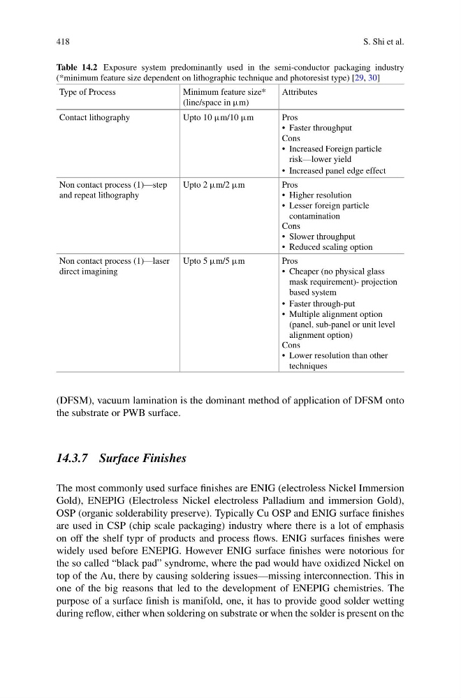
Table 14.2 Exposure system predominantly used in the semi-conductor packaging industry
(*minimum feature size dependent on lithographic technique and photoresist type) [29, 30]
Type of Process
Minimum feature size*
(line/space in μm)
Attributes
Contact lithography
Upto 10 μm/10 μm
Pros
• Faster throughput
Cons
• Increased Foreign particle
risk—lower yield
• Increased panel edge effect
Non contact process (1)—step
and repeat lithography
Upto 2 μm/2 μm
Pros
• Higher resolution
• Lesser foreign particle
contamination
Cons
• Slower throughput
• Reduced scaling option
Non contact process (1)—laser
direct imagining
Upto 5 μm/5 μm
Pros
• Cheaper (no physical glass
mask requirement)- projection
based system
• Faster through-put
• Multiple alignment option
(panel, sub-panel or unit level
alignment option)
Cons
• Lower resolution than other
techniques
(DFSM), vacuum lamination is the dominant method of application of DFSM onto
the substrate or PWB surface.
14.3.7 Surface Finishes
The most commonly used surface finishes are ENIG (electroless Nickel Immersion
Gold), ENEPIG (Electroless Nickel electroless Palladium and immersion Gold),
OSP (organic solderability preserve). Typically Cu OSP and ENIG surface finishes
are used in CSP (chip scale packaging) industry where there is a lot of emphasis
on off the shelf typr of products and process flows. ENIG surfaces finishes were
widely used before ENEPIG. However ENIG surface finishes were notorious for
the so called “black pad” syndrome, where the pad would have oxidized Nickel on
top of the Au, there by causing soldering issues—missing interconnection. This in
one of the big reasons that led to the development of ENEPIG chemistries. The
purpose of a surface finish is manifold, one, it has to provide good solder wetting
during reflow, either when soldering on substrate or when the solder is present on the
S. Shi et al.
Table 14.2 Exposure system predominantly used in the semi-conductor packaging industry
(*minimum feature size dependent on lithographic technique and photoresist type) [29, 30]
Type of Process
Minimum feature size*
(line/space in μm)
Attributes
Contact lithography
Upto 10 μm/10 μm
Pros
• Faster throughput
Cons
• Increased Foreign particle
risk—lower yield
• Increased panel edge effect
Non contact process (1)—step
and repeat lithography
Upto 2 μm/2 μm
Pros
• Higher resolution
• Lesser foreign particle
contamination
Cons
• Slower throughput
• Reduced scaling option
Non contact process (1)—laser
direct imagining
Upto 5 μm/5 μm
Pros
• Cheaper (no physical glass
mask requirement)- projection
based system
• Faster through-put
• Multiple alignment option
(panel, sub-panel or unit level
alignment option)
Cons
• Lower resolution than other
techniques
(DFSM), vacuum lamination is the dominant method of application of DFSM onto
the substrate or PWB surface.
14.3.7 Surface Finishes
The most commonly used surface finishes are ENIG (electroless Nickel Immersion
Gold), ENEPIG (Electroless Nickel electroless Palladium and immersion Gold),
OSP (organic solderability preserve). Typically Cu OSP and ENIG surface finishes
are used in CSP (chip scale packaging) industry where there is a lot of emphasis
on off the shelf typr of products and process flows. ENIG surfaces finishes were
widely used before ENEPIG. However ENIG surface finishes were notorious for
the so called “black pad” syndrome, where the pad would have oxidized Nickel on
top of the Au, there by causing soldering issues—missing interconnection. This in
one of the big reasons that led to the development of ENEPIG chemistries. The
purpose of a surface finish is manifold, one, it has to provide good solder wetting
during reflow, either when soldering on substrate or when the solder is present on the