

316
S. Lee
Table 10.11 Resistance
variation of reflow- and
TCB-processed flip-chip
packages upon EM-aging test
at 135 °C under the applied
current of 3 × 10 4 A/cm 2
Time (min)
Resistance ()
MR
TCB
0
0.600
0.667
1
0.600
0.687
25
0.610
0.717
27
0.613
0.780
28
0.617
Failed
50
0.623
51
Failed
Note that the initial resistance value for TCB solder joints, 0.667 ,
is higher than that for reflow solder joints, 0.600
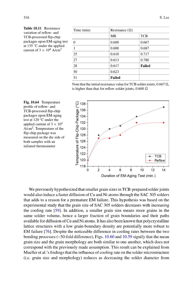
Fig. 10.64 Temperature
profile of reflow- and
TCB-processed flip-chip
packages upon EM-aging
test at 120 °C under the
applied current of 3 × 10 4
A/cm 2 . Temperature of the
flip-chip package was
measured on the die side of
both samples with an
infrared thermometer
We previously hypothesized that smaller grain sizes in TCB-prepared solder joints
would also induce a faster diffusion of Cu and Ni atoms through the SAC 305 solders
that adds to a reason for a premature EM failure. This hypothesis was based on the
experimental study that the grain size of SAC 305 solders decreases with increasing
the cooling rate [59]. In addition, a smaller grain size means more grains in the
same solder volume, hence a larger fraction of grain boundaries and their paths
available for diffusion of Cu and Ni atoms. It has also been known that polycrystalline
lattice structures with a low grain-boundary density are potentially more robust to
EM failure [76]. Despite the noticeable difference in cooling rates between the two
bonding processes (~30-fold difference), Figs. 10.60 and 10.59 signify that the mean
grain size and the grain morphology are both similar to one another, which does not
correspond with the previously made assumption. This result can be explained from
Mueller et al.’s findings that the influence of cooling rate on the solder microstructure
(i.e. grain size and morphology) reduces as decreasing the solder diameter from
S. Lee
Table 10.11 Resistance
variation of reflow- and
TCB-processed flip-chip
packages upon EM-aging test
at 135 °C under the applied
current of 3 × 10 4 A/cm 2
Time (min)
Resistance ()
MR
TCB
0
0.600
0.667
1
0.600
0.687
25
0.610
0.717
27
0.613
0.780
28
0.617
Failed
50
0.623
51
Failed
Note that the initial resistance value for TCB solder joints, 0.667 ,
is higher than that for reflow solder joints, 0.600
Fig. 10.64 Temperature
profile of reflow- and
TCB-processed flip-chip
packages upon EM-aging
test at 120 °C under the
applied current of 3 × 10 4
A/cm 2 . Temperature of the
flip-chip package was
measured on the die side of
both samples with an
infrared thermometer
We previously hypothesized that smaller grain sizes in TCB-prepared solder joints
would also induce a faster diffusion of Cu and Ni atoms through the SAC 305 solders
that adds to a reason for a premature EM failure. This hypothesis was based on the
experimental study that the grain size of SAC 305 solders decreases with increasing
the cooling rate [59]. In addition, a smaller grain size means more grains in the
same solder volume, hence a larger fraction of grain boundaries and their paths
available for diffusion of Cu and Ni atoms. It has also been known that polycrystalline
lattice structures with a low grain-boundary density are potentially more robust to
EM failure [76]. Despite the noticeable difference in cooling rates between the two
bonding processes (~30-fold difference), Figs. 10.60 and 10.59 signify that the mean
grain size and the grain morphology are both similar to one another, which does not
correspond with the previously made assumption. This result can be explained from
Mueller et al.’s findings that the influence of cooling rate on the solder microstructure
(i.e. grain size and morphology) reduces as decreasing the solder diameter from