

306
S. Lee
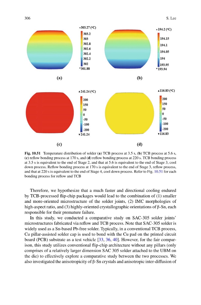
Fig. 10.51 Temperature distribution of solder (a) TCB process at 3.5 s, (b) TCB process at 5.6 s,
(c) reflow bonding process at 170 s, and (d) reflow bonding process at 220 s. TCB bonding process
at 3.5 s is equivalent to the end of Stage 2, and that at 5.6 is equivalent to the end of Stage 3, cool
down process. Reflow bonding process at 170 s is equivalent to the end of Stage 3, reflow process,
and that at 220 s is equivalent to the end of Stage 4, cool down process. Refer to Fig. 10.51 for each
bonding process for reflow and TCB
Therefore, we hypothesize that a much faster and directional cooling endured
by TCB-processed flip-chip packages would lead to the combination of (1) smaller
and more-oriented microstructure of the solder joints, (2) IMC morphologies of
high-aspect ratio, and (3) highly-oriented crystallographic orientations of β-Sn, each
responsible for their premature failure.
In this study, we conducted a comparative study on SAC-305 solder joints’
microstructures fabricated via reflow and TCB process. Note that SAC-305 solder is
widely used as a Sn-based Pb-free solder. Typically, in a conventional TCB process,
Cu pillar-assisted solder cap is used to bond with the Cu pad on the printed circuit
board (PCB) substrate as a test vehicle [33, 36, 40]. However, for the fair comparison, this study utilizes conventional flip-chip architecture without any pillars (only
comprises of a relatively larger dimension SAC 305 solder attached to the UBM on
the die) to effectively explore a comparative study between the two processes. We
also investigated the anisotropicity of β-Sn crystals and anisotropic inter-diffusion of
S. Lee
Fig. 10.51 Temperature distribution of solder (a) TCB process at 3.5 s, (b) TCB process at 5.6 s,
(c) reflow bonding process at 170 s, and (d) reflow bonding process at 220 s. TCB bonding process
at 3.5 s is equivalent to the end of Stage 2, and that at 5.6 is equivalent to the end of Stage 3, cool
down process. Reflow bonding process at 170 s is equivalent to the end of Stage 3, reflow process,
and that at 220 s is equivalent to the end of Stage 4, cool down process. Refer to Fig. 10.51 for each
bonding process for reflow and TCB
Therefore, we hypothesize that a much faster and directional cooling endured
by TCB-processed flip-chip packages would lead to the combination of (1) smaller
and more-oriented microstructure of the solder joints, (2) IMC morphologies of
high-aspect ratio, and (3) highly-oriented crystallographic orientations of β-Sn, each
responsible for their premature failure.
In this study, we conducted a comparative study on SAC-305 solder joints’
microstructures fabricated via reflow and TCB process. Note that SAC-305 solder is
widely used as a Sn-based Pb-free solder. Typically, in a conventional TCB process,
Cu pillar-assisted solder cap is used to bond with the Cu pad on the printed circuit
board (PCB) substrate as a test vehicle [33, 36, 40]. However, for the fair comparison, this study utilizes conventional flip-chip architecture without any pillars (only
comprises of a relatively larger dimension SAC 305 solder attached to the UBM on
the die) to effectively explore a comparative study between the two processes. We
also investigated the anisotropicity of β-Sn crystals and anisotropic inter-diffusion of