

182
H. Ma et al.
liquid into a mixture of liquid droplets and vapor which are then ejected from the
target [75–79].
It is important to consider the ILD stack layers, material properties and thickness
prior to selecting the right laser systems (wavelength, pulse duration and frequency) to
ensure scribe and singulation quality is acceptable for reliability and yield. Although
historically, UV nanosecond laser is used for scribing and singulation, it can become
a challenge to maintain similar yield and reliability standard of processing future
advance low-k and stack complexity. This may require shorter pulse duration or
ultrafast laser system or any other novel technology such as stealth dicing, plasma
singulation or laser water jet. The interaction of ultrafast laser pulses with a target
material happens at a small time scale (picosecond or less) and a small spatial scale
along the laser beam irradiation direction (tens of nanometers), accompanied with
strong nonlinear, non-equilibrium, optically, thermally, and mechanically coupled
processes [80]. Since the ablation mechanism is non-linear, the energy coupling
during ablation of a multi stack low-k layers is highly efficient compared to nanosecond laser.
7.6 Wafer Saw Process
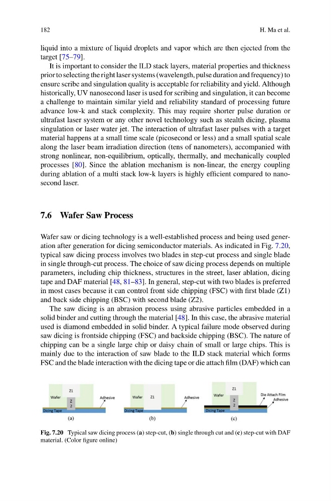
Wafer saw or dicing technology is a well-established process and being used generation after generation for dicing semiconductor materials. As indicated in Fig. 7.20,
typical saw dicing process involves two blades in step-cut process and single blade
in single through-cut process. The choice of saw dicing process depends on multiple
parameters, including chip thickness, structures in the street, laser ablation, dicing
tape and DAF material [48, 81–83]. In general, step-cut with two blades is preferred
in most cases because it can control front side chipping (FSC) with first blade (Z1)
and back side chipping (BSC) with second blade (Z2).
The saw dicing is an abrasion process using abrasive particles embedded in a
solid binder and cutting through the material [48]. In this case, the abrasive material
used is diamond embedded in solid binder. A typical failure mode observed during
saw dicing is frontside chipping (FSC) and backside chipping (BSC). The nature of
chipping can be a single large chip or daisy chain of small or large chips. This is
mainly due to the interaction of saw blade to the ILD stack material which forms
FSC and the blade interaction with the dicing tape or die attach film (DAF) which can
Fig. 7.20 Typical saw dicing process (a) step-cut, (b) single through cut and (c) step-cut with DAF
material. (Color figure online)
H. Ma et al.
liquid into a mixture of liquid droplets and vapor which are then ejected from the
target [75–79].
It is important to consider the ILD stack layers, material properties and thickness
prior to selecting the right laser systems (wavelength, pulse duration and frequency) to
ensure scribe and singulation quality is acceptable for reliability and yield. Although
historically, UV nanosecond laser is used for scribing and singulation, it can become
a challenge to maintain similar yield and reliability standard of processing future
advance low-k and stack complexity. This may require shorter pulse duration or
ultrafast laser system or any other novel technology such as stealth dicing, plasma
singulation or laser water jet. The interaction of ultrafast laser pulses with a target
material happens at a small time scale (picosecond or less) and a small spatial scale
along the laser beam irradiation direction (tens of nanometers), accompanied with
strong nonlinear, non-equilibrium, optically, thermally, and mechanically coupled
processes [80]. Since the ablation mechanism is non-linear, the energy coupling
during ablation of a multi stack low-k layers is highly efficient compared to nanosecond laser.
7.6 Wafer Saw Process
Wafer saw or dicing technology is a well-established process and being used generation after generation for dicing semiconductor materials. As indicated in Fig. 7.20,
typical saw dicing process involves two blades in step-cut process and single blade
in single through-cut process. The choice of saw dicing process depends on multiple
parameters, including chip thickness, structures in the street, laser ablation, dicing
tape and DAF material [48, 81–83]. In general, step-cut with two blades is preferred
in most cases because it can control front side chipping (FSC) with first blade (Z1)
and back side chipping (BSC) with second blade (Z2).
The saw dicing is an abrasion process using abrasive particles embedded in a
solid binder and cutting through the material [48]. In this case, the abrasive material
used is diamond embedded in solid binder. A typical failure mode observed during
saw dicing is frontside chipping (FSC) and backside chipping (BSC). The nature of
chipping can be a single large chip or daisy chain of small or large chips. This is
mainly due to the interaction of saw blade to the ILD stack material which forms
FSC and the blade interaction with the dicing tape or die attach film (DAF) which can
Fig. 7.20 Typical saw dicing process (a) step-cut, (b) single through cut and (c) step-cut with DAF
material. (Color figure online)