

Solid State Physics
291
saw. The surface of the slice is polished mechanically and chemically, to give
what is referred to as the substrate.
In the next step, a mixture of silicon tetrachloride, hydrogen and phosphine
(PH 3 ) is passed over the substrate at about 1200°C. The silicon released by the
reduction of silicon tetrachloride, along with a suitable amount of phosphorus
(from the PH 3 ), crystallizes on the substrate surface forming what is known as
an n-type epitaxial layer (for producing p-type epitaxial layer PH 3 is replaced
by diborane, B 2 H 6 ).
The surface of the epitaxial layer is oxidized by heating the substrate to
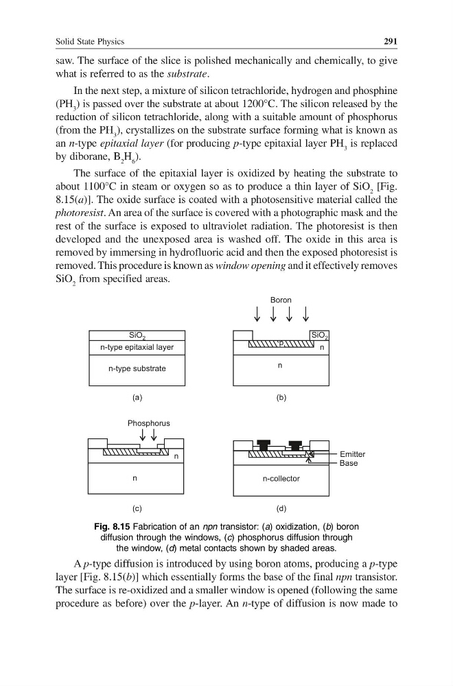
about 1100°C in steam or oxygen so as to produce a thin layer of SiO 2 [Fig.
8.15(a)]. The oxide surface is coated with a photosensitive material called the
photoresist. An area of the surface is covered with a photographic mask and the
rest of the surface is exposed to ultraviolet radiation. The photoresist is then
developed and the unexposed area is washed off. The oxide in this area is
removed by immersing in hydrofluoric acid and then the exposed photoresist is
removed. This procedure is known as window opening and it effectively removes
SiO 2 from specified areas.
SiO 2
n-type epitaxial layer
n-type substrate
(a)
SiO 2
n
n
Boron
(b)
Phosphorus
(c)
(d)
n
n
Emitter
Base
n-collector
p
Fig. 8.15 Fabrication of an npn transistor: (a) oxidization, (b) boron
diffusion through the windows, (c) phosphorus diffusion through
the window, (d) metal contacts shown by shaded areas.
A p-type diffusion is introduced by using boron atoms, producing a p-type
layer [Fig. 8.15(b)] which essentially forms the base of the final npn transistor.
The surface is re-oxidized and a smaller window is opened (following the same
procedure as before) over the p-layer. An n-type of diffusion is now made to
291
saw. The surface of the slice is polished mechanically and chemically, to give
what is referred to as the substrate.
In the next step, a mixture of silicon tetrachloride, hydrogen and phosphine
(PH 3 ) is passed over the substrate at about 1200°C. The silicon released by the
reduction of silicon tetrachloride, along with a suitable amount of phosphorus
(from the PH 3 ), crystallizes on the substrate surface forming what is known as
an n-type epitaxial layer (for producing p-type epitaxial layer PH 3 is replaced
by diborane, B 2 H 6 ).
The surface of the epitaxial layer is oxidized by heating the substrate to
about 1100°C in steam or oxygen so as to produce a thin layer of SiO 2 [Fig.
8.15(a)]. The oxide surface is coated with a photosensitive material called the
photoresist. An area of the surface is covered with a photographic mask and the
rest of the surface is exposed to ultraviolet radiation. The photoresist is then
developed and the unexposed area is washed off. The oxide in this area is
removed by immersing in hydrofluoric acid and then the exposed photoresist is
removed. This procedure is known as window opening and it effectively removes
SiO 2 from specified areas.
SiO 2
n-type epitaxial layer
n-type substrate
(a)
SiO 2
n
n
Boron
(b)
Phosphorus
(c)
(d)
n
n
Emitter
Base
n-collector
p
Fig. 8.15 Fabrication of an npn transistor: (a) oxidization, (b) boron
diffusion through the windows, (c) phosphorus diffusion through
the window, (d) metal contacts shown by shaded areas.
A p-type diffusion is introduced by using boron atoms, producing a p-type
layer [Fig. 8.15(b)] which essentially forms the base of the final npn transistor.
The surface is re-oxidized and a smaller window is opened (following the same
procedure as before) over the p-layer. An n-type of diffusion is now made to