

86
W. C. Law and S. De W. Wong
A set of optically aligned grids (Mo, W, graphite) acts as electrostatic aperture, which
extracts and accelerates the ions to form a mono-energetic collimated beam. The inner
grid (screen grid) is biased positive relative to the beam voltage, while the center
grid (accelerator grid) is biased negative relative to the acceleration voltage, creating
an electric field due to the potential difference. Ions in the plasma are extracted
through the apertures and accelerated away from the source at high energies (300–
1000 eV). The outer grid (decelerator grid) is placed at ground potential, which acts
a collimator to reduce the beam divergence and also prevent the back-streaming of
electrons from the plasma bridge neutralizer. The plasma bridge neutralizer emits
electrons orthogonal to the grids to neutralize the incoming charged ion beam, and
hence prevents space or surface charging of the sample. A secondary ions mass
spectroscopy (SIMS) detector collects the ejected secondary ions from the sample to
obtain the elemental composition of the etched materials and also provide a real-time
end point detection system.
6.5.3 Prevailing Challenges
Non-volatile By-products.
Typically, plasma etching is based on the volatility of the etched by-products. Due
to the thermodynamically-favored reaction, there is no ion bombardment necessary
during etching, but only to induce directionality. The optimum photoresist sidewall
is slightly sloped at 86°−88° for good device pitch and size control. However, the
aggressive etching process of plasma etching requires the utilization of a hard mask
that can tolerate long etch time or high bias power. The hard mask is etched with
photoresist patterns, then the photoresist is stripped away and the etching of the MTJ
is continued with the hard mask only. Si is easily etched by halogen etch chemistries,
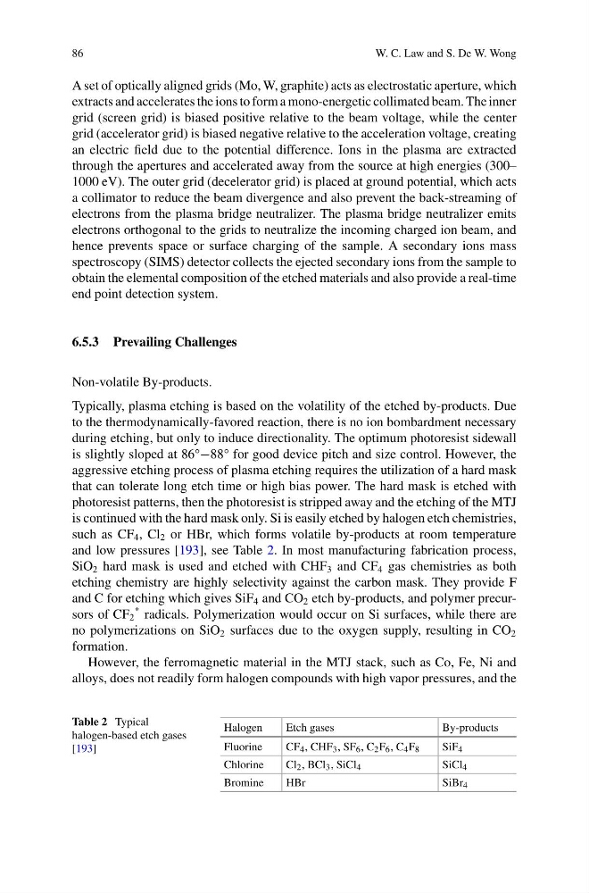
such as CF 4 , Cl 2 or HBr, which forms volatile by-products at room temperature
and low pressures [193], see Table 2. In most manufacturing fabrication process,
SiO 2 hard mask is used and etched with CHF 3 and CF 4 gas chemistries as both
etching chemistry are highly selectivity against the carbon mask. They provide F
and C for etching which gives SiF 4 and CO 2 etch by-products, and polymer precursors of CF 2
* radicals. Polymerization would occur on Si surfaces, while there are
no polymerizations on SiO 2 surfaces due to the oxygen supply, resulting in CO 2
formation.
However, the ferromagnetic material in the MTJ stack, such as Co, Fe, Ni and
alloys, does not readily form halogen compounds with high vapor pressures, and the
Table 2 Typical
halogen-based etch gases
[193]
Halogen
Etch gases
By-products
Fluorine
CF 4 , CHF 3 , SF 6 , C 2 F 6 , C 4 F 8
SiF 4
Chlorine
Cl 2 , BCl 3 , SiCl 4
SiCl 4
Bromine
HBr
SiBr 4
W. C. Law and S. De W. Wong
A set of optically aligned grids (Mo, W, graphite) acts as electrostatic aperture, which
extracts and accelerates the ions to form a mono-energetic collimated beam. The inner
grid (screen grid) is biased positive relative to the beam voltage, while the center
grid (accelerator grid) is biased negative relative to the acceleration voltage, creating
an electric field due to the potential difference. Ions in the plasma are extracted
through the apertures and accelerated away from the source at high energies (300–
1000 eV). The outer grid (decelerator grid) is placed at ground potential, which acts
a collimator to reduce the beam divergence and also prevent the back-streaming of
electrons from the plasma bridge neutralizer. The plasma bridge neutralizer emits
electrons orthogonal to the grids to neutralize the incoming charged ion beam, and
hence prevents space or surface charging of the sample. A secondary ions mass
spectroscopy (SIMS) detector collects the ejected secondary ions from the sample to
obtain the elemental composition of the etched materials and also provide a real-time
end point detection system.
6.5.3 Prevailing Challenges
Non-volatile By-products.
Typically, plasma etching is based on the volatility of the etched by-products. Due
to the thermodynamically-favored reaction, there is no ion bombardment necessary
during etching, but only to induce directionality. The optimum photoresist sidewall
is slightly sloped at 86°−88° for good device pitch and size control. However, the
aggressive etching process of plasma etching requires the utilization of a hard mask
that can tolerate long etch time or high bias power. The hard mask is etched with
photoresist patterns, then the photoresist is stripped away and the etching of the MTJ
is continued with the hard mask only. Si is easily etched by halogen etch chemistries,
such as CF 4 , Cl 2 or HBr, which forms volatile by-products at room temperature
and low pressures [193], see Table 2. In most manufacturing fabrication process,
SiO 2 hard mask is used and etched with CHF 3 and CF 4 gas chemistries as both
etching chemistry are highly selectivity against the carbon mask. They provide F
and C for etching which gives SiF 4 and CO 2 etch by-products, and polymer precursors of CF 2
* radicals. Polymerization would occur on Si surfaces, while there are
no polymerizations on SiO 2 surfaces due to the oxygen supply, resulting in CO 2
formation.
However, the ferromagnetic material in the MTJ stack, such as Co, Fe, Ni and
alloys, does not readily form halogen compounds with high vapor pressures, and the
Table 2 Typical
halogen-based etch gases
[193]
Halogen
Etch gases
By-products
Fluorine
CF 4 , CHF 3 , SF 6 , C 2 F 6 , C 4 F 8
SiF 4
Chlorine
Cl 2 , BCl 3 , SiCl 4
SiCl 4
Bromine
HBr
SiBr 4