

50
W. C. Law and S. De W. Wong
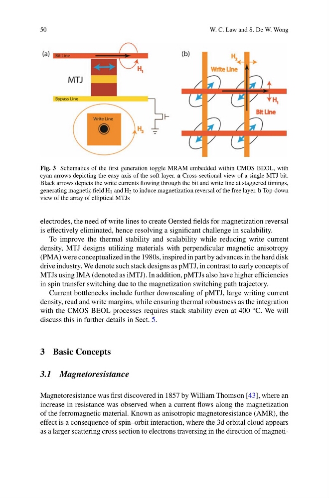
Fig. 3 Schematics of the first generation toggle MRAM embedded within CMOS BEOL, with
cyan arrows depicting the easy axis of the soft layer. a Cross-sectional view of a single MTJ bit.
Black arrows depicts the write currents flowing through the bit and write line at staggered timings,
generating magnetic field H 1 and H 2 to induce magnetization reversal of the free layer. b Top-down
view of the array of elliptical MTJs
electrodes, the need of write lines to create Oersted fields for magnetization reversal
is effectively eliminated, hence resolving a significant challenge in scalability.
To improve the thermal stability and scalability while reducing write current
density, MTJ designs utilizing materials with perpendicular magnetic anisotropy
(PMA) were conceptualized in the 1980s, inspired in part by advances in the hard disk
drive industry. We denote such stack designs as pMTJ, in contrast to early concepts of
MTJs using IMA (denoted as iMTJ). In addition, pMTJs also have higher efficiencies
in spin transfer switching due to the magnetization switching path trajectory.
Current bottlenecks include further downscaling of pMTJ, large writing current
density, read and write margins, while ensuring thermal robustness as the integration
with the CMOS BEOL processes requires stack stability even at 400 °C. We will
discuss this in further details in Sect. 5.
3 Basic Concepts
3.1 Magnetoresistance
Magnetoresistance was first discovered in 1857 by William Thomson [43], where an
increase in resistance was observed when a current flows along the magnetization
of the ferromagnetic material. Known as anisotropic magnetoresistance (AMR), the
effect is a consequence of spin–orbit interaction, where the 3d orbital cloud appears
as a larger scattering cross section to electrons traversing in the direction of magneti-
W. C. Law and S. De W. Wong
Fig. 3 Schematics of the first generation toggle MRAM embedded within CMOS BEOL, with
cyan arrows depicting the easy axis of the soft layer. a Cross-sectional view of a single MTJ bit.
Black arrows depicts the write currents flowing through the bit and write line at staggered timings,
generating magnetic field H 1 and H 2 to induce magnetization reversal of the free layer. b Top-down
view of the array of elliptical MTJs
electrodes, the need of write lines to create Oersted fields for magnetization reversal
is effectively eliminated, hence resolving a significant challenge in scalability.
To improve the thermal stability and scalability while reducing write current
density, MTJ designs utilizing materials with perpendicular magnetic anisotropy
(PMA) were conceptualized in the 1980s, inspired in part by advances in the hard disk
drive industry. We denote such stack designs as pMTJ, in contrast to early concepts of
MTJs using IMA (denoted as iMTJ). In addition, pMTJs also have higher efficiencies
in spin transfer switching due to the magnetization switching path trajectory.
Current bottlenecks include further downscaling of pMTJ, large writing current
density, read and write margins, while ensuring thermal robustness as the integration
with the CMOS BEOL processes requires stack stability even at 400 °C. We will
discuss this in further details in Sect. 5.
3 Basic Concepts
3.1 Magnetoresistance
Magnetoresistance was first discovered in 1857 by William Thomson [43], where an
increase in resistance was observed when a current flows along the magnetization
of the ferromagnetic material. Known as anisotropic magnetoresistance (AMR), the
effect is a consequence of spin–orbit interaction, where the 3d orbital cloud appears
as a larger scattering cross section to electrons traversing in the direction of magneti-