

110
S. Krishnia and W. S. Lew
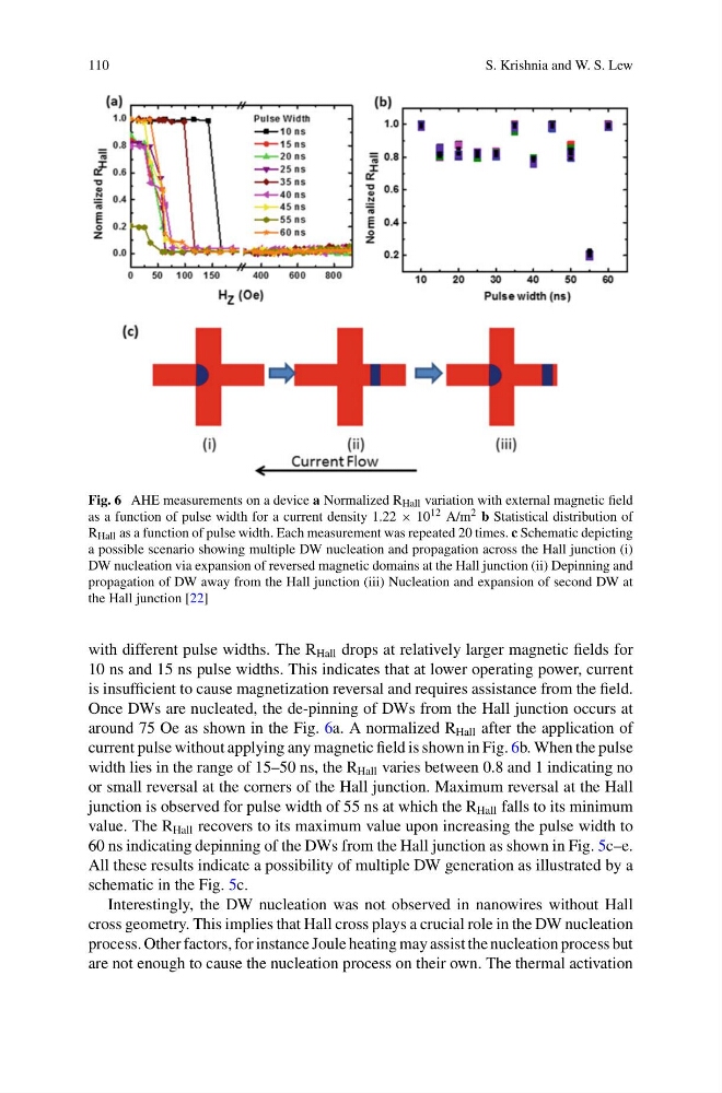
Fig. 6 AHE measurements on a device a Normalized R Hall variation with external magnetic field
as a function of pulse width for a current density 1.22 × 10 12 A/m 2 b Statistical distribution of
R Hall as a function of pulse width. Each measurement was repeated 20 times. c Schematic depicting
a possible scenario showing multiple DW nucleation and propagation across the Hall junction (i)
DW nucleation via expansion of reversed magnetic domains at the Hall junction (ii) Depinning and
propagation of DW away from the Hall junction (iii) Nucleation and expansion of second DW at
the Hall junction [22]
with different pulse widths. The R Hall drops at relatively larger magnetic fields for
10 ns and 15 ns pulse widths. This indicates that at lower operating power, current
is insufficient to cause magnetization reversal and requires assistance from the field.
Once DWs are nucleated, the de-pinning of DWs from the Hall junction occurs at
around 75 Oe as shown in the Fig. 6a. A normalized R Hall after the application of
current pulse without applying any magnetic field is shown in Fig. 6b. When the pulse
width lies in the range of 15–50 ns, the R Hall varies between 0.8 and 1 indicating no
or small reversal at the corners of the Hall junction. Maximum reversal at the Hall
junction is observed for pulse width of 55 ns at which the R Hall falls to its minimum
value. The R Hall recovers to its maximum value upon increasing the pulse width to
60 ns indicating depinning of the DWs from the Hall junction as shown in Fig. 5c–e.
All these results indicate a possibility of multiple DW generation as illustrated by a
schematic in the Fig. 5c.
Interestingly, the DW nucleation was not observed in nanowires without Hall
cross geometry. This implies that Hall cross plays a crucial role in the DW nucleation
process. Other factors, for instance Joule heating may assist the nucleation process but
are not enough to cause the nucleation process on their own. The thermal activation
S. Krishnia and W. S. Lew
Fig. 6 AHE measurements on a device a Normalized R Hall variation with external magnetic field
as a function of pulse width for a current density 1.22 × 10 12 A/m 2 b Statistical distribution of
R Hall as a function of pulse width. Each measurement was repeated 20 times. c Schematic depicting
a possible scenario showing multiple DW nucleation and propagation across the Hall junction (i)
DW nucleation via expansion of reversed magnetic domains at the Hall junction (ii) Depinning and
propagation of DW away from the Hall junction (iii) Nucleation and expansion of second DW at
the Hall junction [22]
with different pulse widths. The R Hall drops at relatively larger magnetic fields for
10 ns and 15 ns pulse widths. This indicates that at lower operating power, current
is insufficient to cause magnetization reversal and requires assistance from the field.
Once DWs are nucleated, the de-pinning of DWs from the Hall junction occurs at
around 75 Oe as shown in the Fig. 6a. A normalized R Hall after the application of
current pulse without applying any magnetic field is shown in Fig. 6b. When the pulse
width lies in the range of 15–50 ns, the R Hall varies between 0.8 and 1 indicating no
or small reversal at the corners of the Hall junction. Maximum reversal at the Hall
junction is observed for pulse width of 55 ns at which the R Hall falls to its minimum
value. The R Hall recovers to its maximum value upon increasing the pulse width to
60 ns indicating depinning of the DWs from the Hall junction as shown in Fig. 5c–e.
All these results indicate a possibility of multiple DW generation as illustrated by a
schematic in the Fig. 5c.
Interestingly, the DW nucleation was not observed in nanowires without Hall
cross geometry. This implies that Hall cross plays a crucial role in the DW nucleation
process. Other factors, for instance Joule heating may assist the nucleation process but
are not enough to cause the nucleation process on their own. The thermal activation