

108
S. Krishnia and W. S. Lew
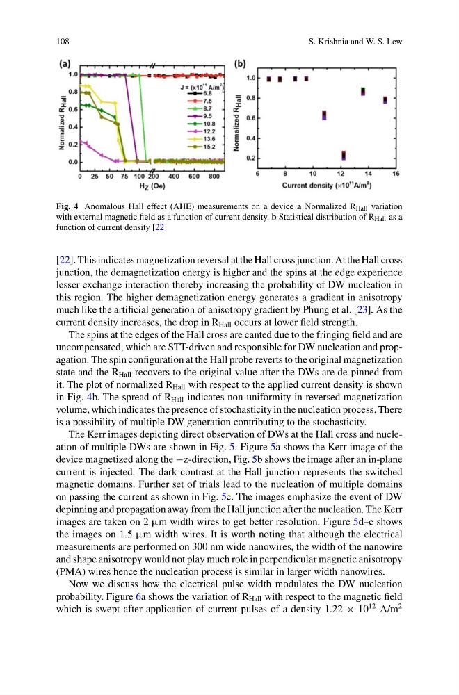
Fig. 4 Anomalous Hall effect (AHE) measurements on a device a Normalized R Hall variation
with external magnetic field as a function of current density. b Statistical distribution of R Hall as a
function of current density [22]
[22]. This indicates magnetization reversal at the Hall cross junction. At the Hall cross
junction, the demagnetization energy is higher and the spins at the edge experience
lesser exchange interaction thereby increasing the probability of DW nucleation in
this region. The higher demagnetization energy generates a gradient in anisotropy
much like the artificial generation of anisotropy gradient by Phung et al. [23]. As the
current density increases, the drop in R Hall occurs at lower field strength.
The spins at the edges of the Hall cross are canted due to the fringing field and are
uncompensated, which are STT-driven and responsible for DW nucleation and propagation. The spin configuration at the Hall probe reverts to the original magnetization
state and the R Hall recovers to the original value after the DWs are de-pinned from
it. The plot of normalized R Hall with respect to the applied current density is shown
in Fig. 4b. The spread of R Hall indicates non-uniformity in reversed magnetization
volume, which indicates the presence of stochasticity in the nucleation process. There
is a possibility of multiple DW generation contributing to the stochasticity.
The Kerr images depicting direct observation of DWs at the Hall cross and nucleation of multiple DWs are shown in Fig. 5. Figure 5a shows the Kerr image of the
device magnetized along the −z-direction, Fig. 5b shows the image after an in-plane
current is injected. The dark contrast at the Hall junction represents the switched
magnetic domains. Further set of trials lead to the nucleation of multiple domains
on passing the current as shown in Fig. 5c. The images emphasize the event of DW
depinning and propagation away from the Hall junction after the nucleation. The Kerr
images are taken on 2 μm width wires to get better resolution. Figure 5d–e shows
the images on 1.5 μm width wires. It is worth noting that although the electrical
measurements are performed on 300 nm wide nanowires, the width of the nanowire
and shape anisotropy would not play much role in perpendicular magnetic anisotropy
(PMA) wires hence the nucleation process is similar in larger width nanowires.
Now we discuss how the electrical pulse width modulates the DW nucleation
probability. Figure 6a shows the variation of R Hall with respect to the magnetic field
which is swept after application of current pulses of a density 1.22 × 10
12 A/m
2
S. Krishnia and W. S. Lew
Fig. 4 Anomalous Hall effect (AHE) measurements on a device a Normalized R Hall variation
with external magnetic field as a function of current density. b Statistical distribution of R Hall as a
function of current density [22]
[22]. This indicates magnetization reversal at the Hall cross junction. At the Hall cross
junction, the demagnetization energy is higher and the spins at the edge experience
lesser exchange interaction thereby increasing the probability of DW nucleation in
this region. The higher demagnetization energy generates a gradient in anisotropy
much like the artificial generation of anisotropy gradient by Phung et al. [23]. As the
current density increases, the drop in R Hall occurs at lower field strength.
The spins at the edges of the Hall cross are canted due to the fringing field and are
uncompensated, which are STT-driven and responsible for DW nucleation and propagation. The spin configuration at the Hall probe reverts to the original magnetization
state and the R Hall recovers to the original value after the DWs are de-pinned from
it. The plot of normalized R Hall with respect to the applied current density is shown
in Fig. 4b. The spread of R Hall indicates non-uniformity in reversed magnetization
volume, which indicates the presence of stochasticity in the nucleation process. There
is a possibility of multiple DW generation contributing to the stochasticity.
The Kerr images depicting direct observation of DWs at the Hall cross and nucleation of multiple DWs are shown in Fig. 5. Figure 5a shows the Kerr image of the
device magnetized along the −z-direction, Fig. 5b shows the image after an in-plane
current is injected. The dark contrast at the Hall junction represents the switched
magnetic domains. Further set of trials lead to the nucleation of multiple domains
on passing the current as shown in Fig. 5c. The images emphasize the event of DW
depinning and propagation away from the Hall junction after the nucleation. The Kerr
images are taken on 2 μm width wires to get better resolution. Figure 5d–e shows
the images on 1.5 μm width wires. It is worth noting that although the electrical
measurements are performed on 300 nm wide nanowires, the width of the nanowire
and shape anisotropy would not play much role in perpendicular magnetic anisotropy
(PMA) wires hence the nucleation process is similar in larger width nanowires.
Now we discuss how the electrical pulse width modulates the DW nucleation
probability. Figure 6a shows the variation of R Hall with respect to the magnetic field
which is swept after application of current pulses of a density 1.22 × 10
12 A/m
2