

9. A bottom chamber is compartmentalized by placing the chip
on the support platform, which is mounted on gold-coated
glass serving as the bottom electrode.
10. The transfection reagents to be injected are filled into the
bottom chamber.
11. All components are stacked on a PMMA substrate with two
clamps.
3.2 Magnetic
Tweezers
1. LOR 2A and S1813 are sequentially spin-coated on 3D
NEP chip.
2. EVG 620 is used to pattern 15 μm diameter circle arrays into
the resist with spacing equivalent to the nanopores.
3. A 50 nm layer of permalloy is deposited onto the entire silicon
surface by sputtering.
4. Lift off permalloy and photoresist.
5. Then fabrication of the pores on the chip (as described in
Subheading 3.1) requires careful alignment of the etching of
nanopores adjacent to the magnetic disk (see Note 3).
6. Using PECVD deposition, the chip is coated with a thin
(~200 nm) layer of SiO 2 (see Note 3).
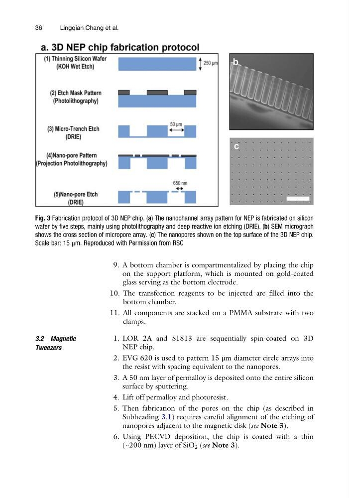
Fig. 3 Fabrication protocol of 3D NEP chip. (a) The nanochannel array pattern for NEP is fabricated on silicon
wafer by five steps, mainly using photolithography and deep reactive ion etching (DRIE). (b) SEM micrograph
shows the cross section of micropore array. (c) The nanopores shown on the top surface of the 3D NEP chip.
Scale bar: 15 μm. Reproduced with Permission from RSC
36
Lingqian Chang et al.
on the support platform, which is mounted on gold-coated
glass serving as the bottom electrode.
10. The transfection reagents to be injected are filled into the
bottom chamber.
11. All components are stacked on a PMMA substrate with two
clamps.
3.2 Magnetic
Tweezers
1. LOR 2A and S1813 are sequentially spin-coated on 3D
NEP chip.
2. EVG 620 is used to pattern 15 μm diameter circle arrays into
the resist with spacing equivalent to the nanopores.
3. A 50 nm layer of permalloy is deposited onto the entire silicon
surface by sputtering.
4. Lift off permalloy and photoresist.
5. Then fabrication of the pores on the chip (as described in
Subheading 3.1) requires careful alignment of the etching of
nanopores adjacent to the magnetic disk (see Note 3).
6. Using PECVD deposition, the chip is coated with a thin
(~200 nm) layer of SiO 2 (see Note 3).
Fig. 3 Fabrication protocol of 3D NEP chip. (a) The nanochannel array pattern for NEP is fabricated on silicon
wafer by five steps, mainly using photolithography and deep reactive ion etching (DRIE). (b) SEM micrograph
shows the cross section of micropore array. (c) The nanopores shown on the top surface of the 3D NEP chip.
Scale bar: 15 μm. Reproduced with Permission from RSC
36
Lingqian Chang et al.