

is first mixed with the curing agent at a weight ratio of 10 to 1.
After vacuum degassing, the mixed PDMS resin is poured onto
the silicon wafer with the SU-8 mold in a petri dish. The
thickness of the PDMS resin on the mold is around 5 mm.
After a secondary vacuum degassing, the petri dish is placed in
an oven at 60
C for 2 h. The cured PDMS is then peeled off
from the silicon wafer and then is cut into small rectangular
pieces, which are about the size of the microfluidic device
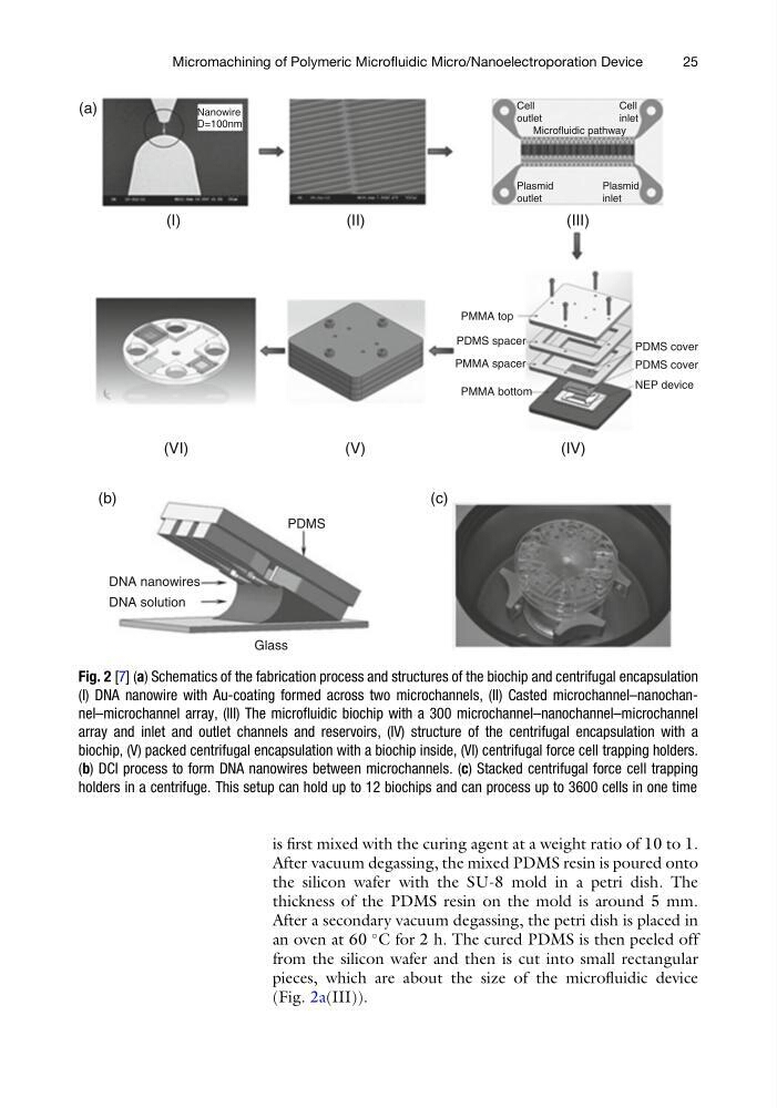
(Fig. 2a(III)).
(a)
(b)
(c)
(I)
Nanowire
Cell
outlet
PMMA top
PDMS cover
PDMS spacer
PDMS
Glass
DNA nanowires
DNA solution
PDMS cover
NEP device
PMMA spacer
PMMA bottom
Plasmid
outlet
Microfluidic pathway
Plasmid
inlet
Cell
inlet
D=100nm
(II)
(III)
(VI)
(V)
(IV)
Fig. 2 [7] (a) Schematics of the fabrication process and structures of the biochip and centrifugal encapsulation
(I) DNA nanowire with Au-coating formed across two microchannels, (II) Casted microchannel–nanochannel–microchannel array, (III) The microfluidic biochip with a 300 microchannel–nanochannel–microchannel
array and inlet and outlet channels and reservoirs, (IV) structure of the centrifugal encapsulation with a
biochip, (V) packed centrifugal encapsulation with a biochip inside, (VI) centrifugal force cell trapping holders.
(b) DCI process to form DNA nanowires between microchannels. (c) Stacked centrifugal force cell trapping
holders in a centrifuge. This setup can hold up to 12 biochips and can process up to 3600 cells in one time
Micromachining of Polymeric Microfluidic Micro/Nanoelectroporation Device
25
After vacuum degassing, the mixed PDMS resin is poured onto
the silicon wafer with the SU-8 mold in a petri dish. The
thickness of the PDMS resin on the mold is around 5 mm.
After a secondary vacuum degassing, the petri dish is placed in
an oven at 60
C for 2 h. The cured PDMS is then peeled off
from the silicon wafer and then is cut into small rectangular
pieces, which are about the size of the microfluidic device
(Fig. 2a(III)).
(a)
(b)
(c)
(I)
Nanowire
Cell
outlet
PMMA top
PDMS cover
PDMS spacer
PDMS
Glass
DNA nanowires
DNA solution
PDMS cover
NEP device
PMMA spacer
PMMA bottom
Plasmid
outlet
Microfluidic pathway
Plasmid
inlet
Cell
inlet
D=100nm
(II)
(III)
(VI)
(V)
(IV)
Fig. 2 [7] (a) Schematics of the fabrication process and structures of the biochip and centrifugal encapsulation
(I) DNA nanowire with Au-coating formed across two microchannels, (II) Casted microchannel–nanochannel–microchannel array, (III) The microfluidic biochip with a 300 microchannel–nanochannel–microchannel
array and inlet and outlet channels and reservoirs, (IV) structure of the centrifugal encapsulation with a
biochip, (V) packed centrifugal encapsulation with a biochip inside, (VI) centrifugal force cell trapping holders.
(b) DCI process to form DNA nanowires between microchannels. (c) Stacked centrifugal force cell trapping
holders in a centrifuge. This setup can hold up to 12 biochips and can process up to 3600 cells in one time
Micromachining of Polymeric Microfluidic Micro/Nanoelectroporation Device
25