

thickness of approximately 100–200 nm should be reached.
Pipettes with a thicker gold coating or a rough surface should
be discarded.
3. Paint pipettes with an additional layer of conductive silver paint
along the shaft in order to obtain sufficient electric conductivity
of the surface to prevent pipettes from overcharging during
application of FIB-mode and to provide better imaging quality
in subsequent imaging steps using SEM-mode.
4. After this pretreatment, coated and painted glass micropipettes
are put in the combined FIB-SEM workstation which is
equipped with a gallium ion source for FIB-mode milling
purposes [10, 11]. We suggest using the gallium-ion gun at
an angle of 90
to the principal axis of the pipette to mill five
square-shaped holes into the glass wall along the shaft, up to an
axial distance of 25 μm from the tip, each set apart by 5 μm.
The size of individual holes needs to decrease with increasing
distance to the tip to account for the axial resistance of the
pipette (see below for more detail). Milling current und dwell
time per area need to be chosen such that every single shot can
penetrate both glass walls leaving behind two openings on
opposite sides of the pipette. This is typically achieved after
1–2 s for small holes and after 10–15 s fort larger holes. Next,
pipettes are rotated axially by 90
and the procedure is
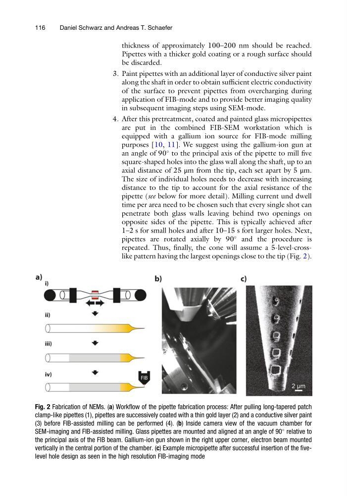
repeated. Thus, finally, the cone will assume a 5-level-crosslike pattern having the largest openings close to the tip (Fig. 2).
Fig. 2 Fabrication of NEMs. (a) Workflow of the pipette fabrication process: After pulling long-tapered patch
clamp-like pipettes (1), pipettes are successively coated with a thin gold layer (2) and a conductive silver paint
(3) before FIB-assisted milling can be performed (4). (b) Inside camera view of the vacuum chamber for
SEM-imaging and FIB-assisted milling. Glass pipettes are mounted and aligned at an angle of 90
relative to
the principal axis of the FIB beam. Gallium-ion gun shown in the right upper corner, electron beam mounted
vertically in the central portion of the chamber. (c) Example micropipette after successful insertion of the fivelevel hole design as seen in the high resolution FIB-imaging mode
116
Daniel Schwarz and Andreas T. Schaefer
Pipettes with a thicker gold coating or a rough surface should
be discarded.
3. Paint pipettes with an additional layer of conductive silver paint
along the shaft in order to obtain sufficient electric conductivity
of the surface to prevent pipettes from overcharging during
application of FIB-mode and to provide better imaging quality
in subsequent imaging steps using SEM-mode.
4. After this pretreatment, coated and painted glass micropipettes
are put in the combined FIB-SEM workstation which is
equipped with a gallium ion source for FIB-mode milling
purposes [10, 11]. We suggest using the gallium-ion gun at
an angle of 90
to the principal axis of the pipette to mill five
square-shaped holes into the glass wall along the shaft, up to an
axial distance of 25 μm from the tip, each set apart by 5 μm.
The size of individual holes needs to decrease with increasing
distance to the tip to account for the axial resistance of the
pipette (see below for more detail). Milling current und dwell
time per area need to be chosen such that every single shot can
penetrate both glass walls leaving behind two openings on
opposite sides of the pipette. This is typically achieved after
1–2 s for small holes and after 10–15 s fort larger holes. Next,
pipettes are rotated axially by 90
and the procedure is
repeated. Thus, finally, the cone will assume a 5-level-crosslike pattern having the largest openings close to the tip (Fig. 2).
Fig. 2 Fabrication of NEMs. (a) Workflow of the pipette fabrication process: After pulling long-tapered patch
clamp-like pipettes (1), pipettes are successively coated with a thin gold layer (2) and a conductive silver paint
(3) before FIB-assisted milling can be performed (4). (b) Inside camera view of the vacuum chamber for
SEM-imaging and FIB-assisted milling. Glass pipettes are mounted and aligned at an angle of 90
relative to
the principal axis of the FIB beam. Gallium-ion gun shown in the right upper corner, electron beam mounted
vertically in the central portion of the chamber. (c) Example micropipette after successful insertion of the fivelevel hole design as seen in the high resolution FIB-imaging mode
116
Daniel Schwarz and Andreas T. Schaefer